Local stress control for CMOS performance enhancement

a local stress and cmos technology, applied in the field of cmos device formation, can solve the problems of limited success, degrading device performance and reliability, etc., and achieve the effect of improving the charge mobility of nmos and pmos devices

Inactive Publication Date: 2005-09-29
TAIWAN SEMICON MFG CO LTD
View PDF13 Cites 92 Cited by
  • Summary
  • Abstract
  • Description
  • Claims
  • Application Information

AI Technical Summary

Benefits of technology

[0008] To achieve the foregoing and other objects, and in accordance with the purposes of the present invention, as embodied and broadly described herein, the present invention provides a semiconductor device and method for forming the same for improving charge mobility in NMOS and PMOS devices simultaneously.

Problems solved by technology

In addition, ion implantation and annealing processes following formation of the gate structure typically introduce additional stresses into the polysilicon gate structure which are translated into the underlying channel region altering device performance.
This approach have met with limited success, however, since the formation the contact etching stop layer, formed with a selected type of stress, e.g., either tensile or compressive degrades device performance of a device of opposite charge carrier polarity (e.g., PMOS, NMOS) which is also covered by the stressed contact etching stop layer.
As a result, the nitride contact etching stop layer is severely damaged, which can have the effect of undesirably changing etching rates and causing unintentional overetching in subsequent processes, for example causing damage to underlying silicon or polysilicon portions of a CMOS device, degrading device performance and reliability.

Method used


Image

  • Local stress control for CMOS performance enhancement
  • Local stress control for CMOS performance enhancement
  • Local stress control for CMOS performance enhancement

Examples


Embodiment Construction

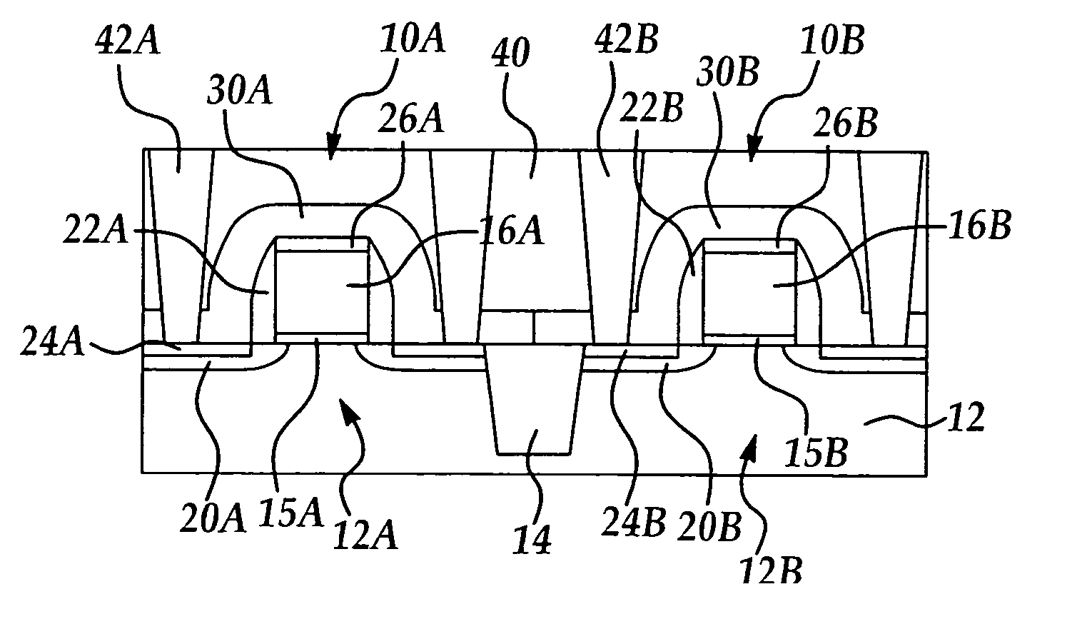
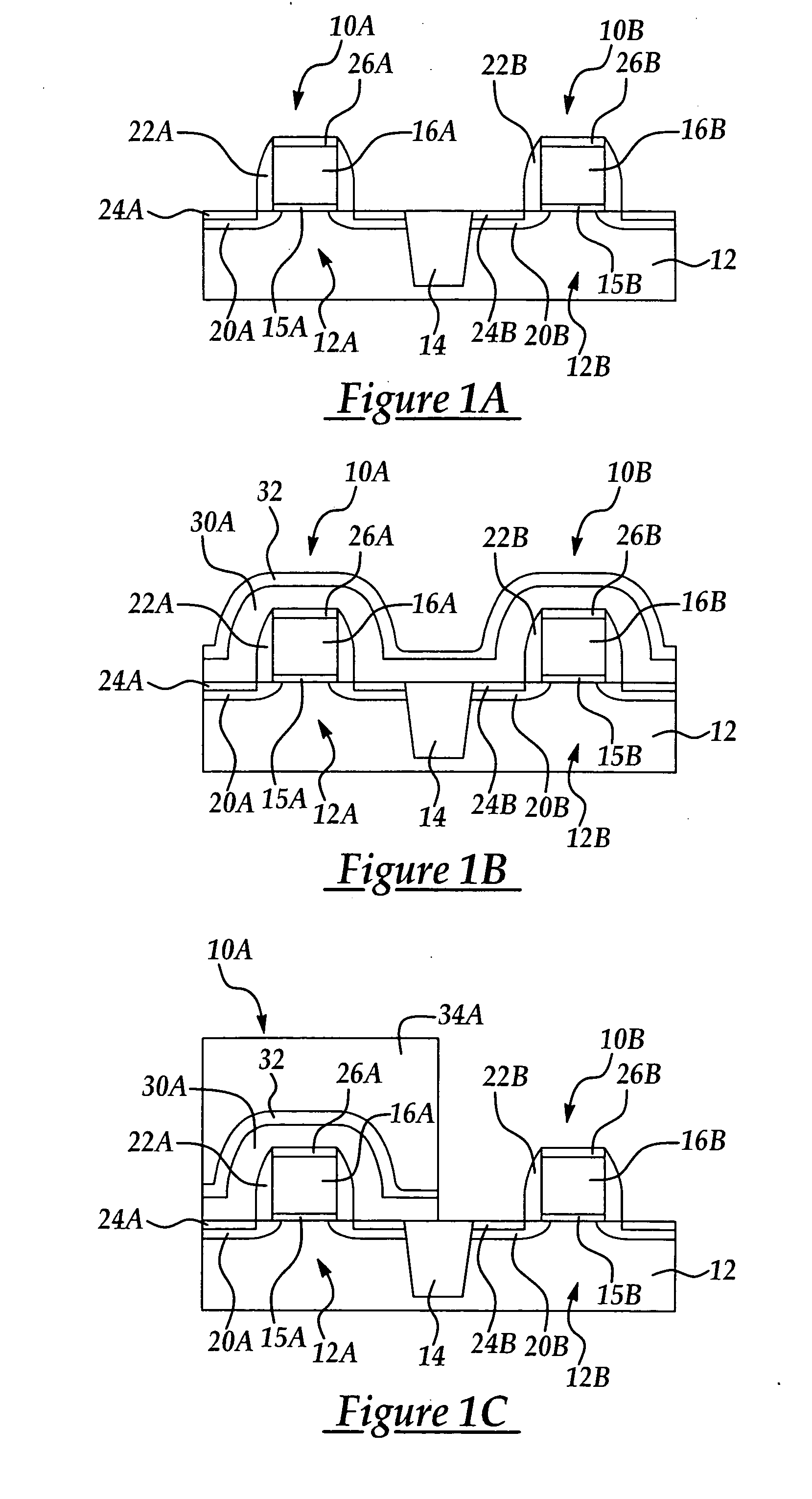
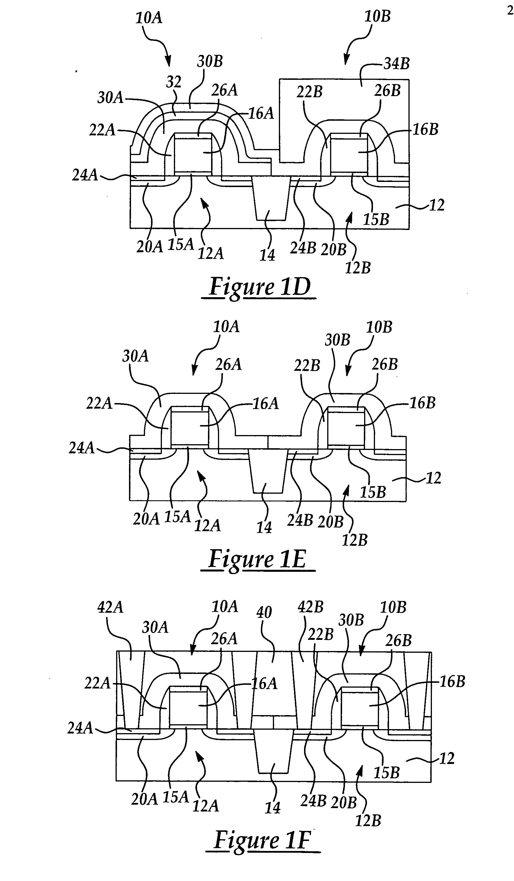
[0013] Although the method of the present invention is explained with reference to an exemplary NMOS and PMOS device pair, it will be appreciated that the method of the present invention may be applied to the formation of any CMOS device where a local tensile and compressive stress is controllably introduced into a respective NMOS and PMOS device region including a channel region to achieve simultaneous device performance improvement including an increase in drive current (Id).

[0014] Referring to FIGS. 1A-1F in an exemplary embodiment of the method of the present invention, are shown cross-sectional schematic views of a portion of a semiconductor wafer during stages in production of CMOS structures including an NMOS and PMOS device pair e.g., 10A and 10B respectively. For example, referring to FIG. 1A is shown a silicon substrate 12 including respective NMOS regions 12A and PMOS region 12B separated by an isolation region, preferably a shallow trench isolation (STI) structure, e.g....


PUM

PropertyMeasurementUnit
thicknessaaaaaaaaaa
tensile stressaaaaaaaaaa
physical thicknessaaaaaaaaaa

Abstract

A semiconductor device and method for forming the same for improving charge mobility in NMOS and PMOS devices simultaneously, the method including forming a first dielectric layer including a stress type selected from the group consisting of tensile stress and compressive stress over the respective PMOS and NMOS device regions; removing a portion of the first dielectric layer overlying one of the PMOS and NMOS device regions; forming a second dielectric layer including a stress type opposite from the first dielectric layer stress type over the respective PMOS and NMOS device regions; and, removing a portion of the second dielectric layer overlying one of the PMOS and NMOS device regions having an underlying first dielectric layer to form a compressive stress dielectric layer over the PMOS device region and a tensile stress dielectric layer over the NMOS device region.

Description

FIELD OF THE INVENTION [0001] This invention generally relates to formation of CMOS devices in integrated circuit manufacturing processes and more particularly to a CMOS device and method that simultaneously achieves mechanically stressed enhanced device performance for both PMOS and NMOS devices. BACKGROUND OF THE INVENTION [0002] Mechanical stresses are known to play a role in charge carrier mobility which affects Voltage threshold and drive current (Id). The effect of induced strain in a channel region of a CMOS device by mechanical stresses affects several critical device performance characteristics including drive current (Id) and particularly drive current saturation levels (IDsat), believed to be related to alteration in charge carrier mobility related to by complex physical processes such as acoustic and optical phonon scattering. [0003] Generally, manufacturing processes are known to introduce stress into the CMOS device channel region. For example, stress is typically intr...

Claims


Application Information

Patent Timeline
Patent Type & Authority Applications(United States)
IPC IPC(8): H01L21/44H01L21/768H01L21/8238
CPCH01L21/76829H01L29/7843H01L21/823828H01L21/823807
Inventor CHEN, CHIEN-HAOCHEN, CHIA-LINLEE, TZE-LIANGCHEN, SHIH-CHANG
Owner TAIWAN SEMICON MFG CO LTD
Why Eureka
Try Eureka