

Semiconductor BGA package having a segmented voltage plane and method of making
a technology of segmented voltage planes and semiconductors, applied in the field of structures, can solve the problems of increasing the number of problems of additional problems, creating thermal and electrical problems, and unique problems of packaging memory devices
- Summary
- Abstract
- Description
- Claims
- Application Information
AI Technical Summary
Benefits of technology
Problems solved by technology
Method used
Image

Examples
Embodiment Construction
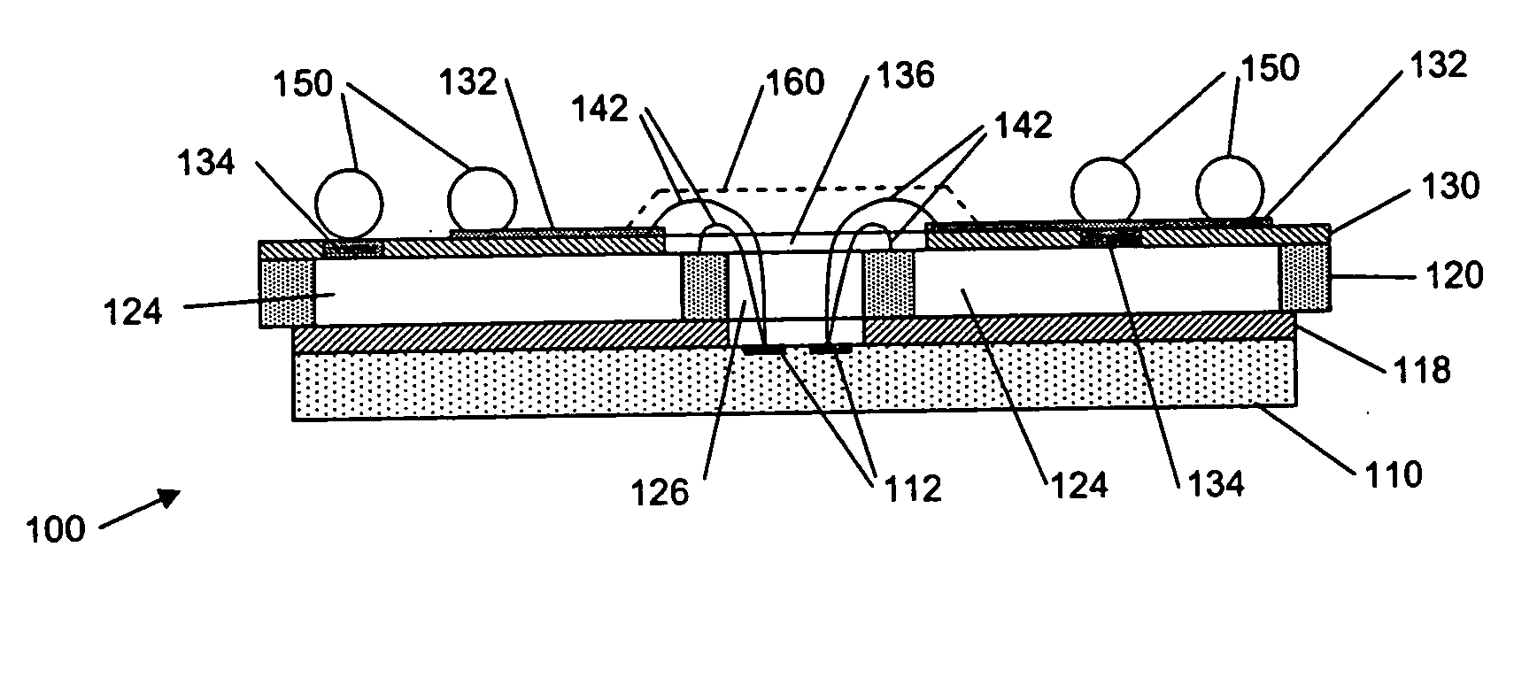
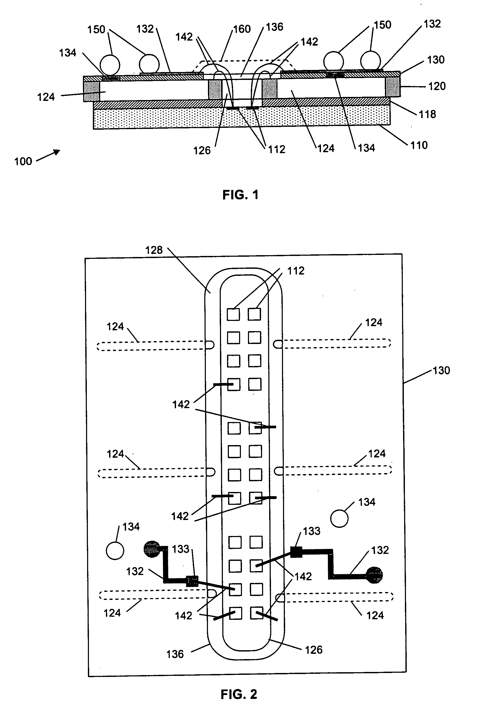
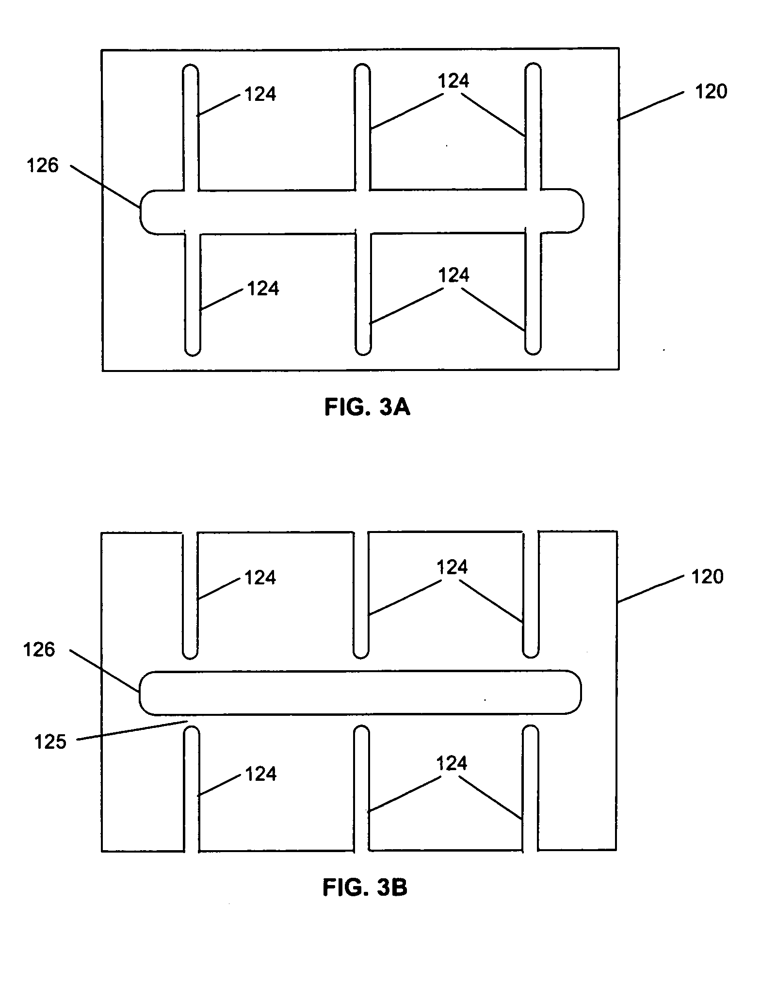
[0023] One exemplary embodiment of the invention is a semiconductor device assembly 100 shown in FIG. 1. This embodiment includes a semiconductor die 110 with a plurality of bond pads 112 on the active surface thereof arranged in two parallel rows adjacent the center of the semiconductor die 110. A thermally conductive dielectric adhesive layer 118 attaches the semiconductor die 110 to an electrically conductive layer 120. The electrically conductive layer 120 includes a longitudinal slot 126 formed along the center of the electrically conductive layer 120 and traversing lengthwise such that the bond pads 112 on the semiconductor die 110 are exposed through the longitudinal slot 126. As shown in FIG. 2, the electrically conductive layer 120 also includes a plurality of electrical current isolation slots 124 therethrough. The electrically conductive layer 120 performs multiple functions. In one aspect, it is of sufficient rigidity to act as a structural support for the semiconductor ...
PUM
 Abstract
Description
Claims
Application Information