Bulk acoustic wave resonator, filter and duplexer and methods of making same

a piezoelectric vibrator and acoustic wave technology, applied in the direction of generators/motors, packaging, transportation and packaging, etc., can solve the problems of increasing the cost and complexity of fabrication, limiting the type, use and timing of cavity etching materials, and acoustically isolating the resonator structure can be a challenge, so as to facilitate electrical connections and improve resonation. , the effect of maximizing the density of the devi

Active Publication Date: 2005-10-06
SAMSUNG ELECTRONICS CO LTD
View PDF23 Cites 51 Cited by
  • Summary
  • Abstract
  • Description
  • Claims
  • Application Information

AI Technical Summary

Benefits of technology

[0009] A resonator in accordance with a first embodiment of the invention includes a support structure, a first electrode located adjacent to a first surface of the support structure, a piezoelectric layer located adjacent to the first electrode and the first surface of the support structure, and a second electrode located adjacent to the piezoelectric layer on a side of the piezoelectric layer opposite to and in electrical isolation from the first electrode. The first electrode, the piezoelectric layer and the second electrode collectively constitute a resonator membrane structure. The support structure includes a cavity that extends from a second surface of the support structure, through the support structure and to a surface of the first electrode closest to the support structure such that at least part of said membrane structure is in acoustic isolation and over said cavity. In this embodiment, the cavity has walls that are substantially parallel to each other and perpendicular to the bottom or second surface of the support structure, i.e., the walls form an angle relative to the second surface of the support structure of 80° to 100°. In this way, device density can be maximized. In certain embodiments, the support structure may be thinner at locations of the substantially parallel-walled cavities. Also, a cap can be applied before the etching of the cavity, with a result of the membrane being less likely to be fouled by debris.
[0010] In a second embodiment, the cavity is formed under the resonator membrane structure using one or more vias extending from the cavity to the bottom or second surface of the support structure. This embodiment avoids the problems associated with placing vias through the front face of the piezoelectric layer and does not necessarily require rigorous side-sided alignment, particularly when etch delimiting layers are utilized. In this embodiment too, a cap can be applied before the etching of the cavity, with a result of the membrane being less likely to be fouled by debris.
[0011] In a third embodiment, a resonator includes a support structure in which a cavity extends from a first surface to a second surface of the support structure. A piezoelectric layer is located adjacent to the first surface of the support structure. A first electrode is located adjacent to the piezoelectric layer coextensive with the cavity and on at least a portion of a wall of the cavity in the support structure. A second electrode is located adjacent to the piezoelectric layer on a side of the piezoelectric layer opposite to and in electrical isolation from said first electrode. The first electrode, the piezoelectric layer and the second electrode form a resonant membrane structure. This embodiment facilitates electrical connections to the electrodes of the resonator membrane structure on the back surface of the support structure and allows the piezoelectric layer to be formed as a continuous layer without a step in the surface in the membrane, making the piezoelectric layer a better resonator.

Problems solved by technology

Acoustically isolating the resonator structure can be a challenge, however.
There are several apparent problems with this technique.
Second, in certain embodiments, additional layers of etch stopping or delimiting materials 726 add to the cost and complexity of fabrication.
Third, because adjacent circuit elements on the same wafer might be present in monolithic integrated circuits, there are limitations on the type, use and timing of the cavity etching material.
Fourth, the etching process must be done before a protective cap can be applied.
This process, however, means that the device density is low.
Additionally, this approach requires that the cavity be aligned on one side with a resonator structure on the other side, and two-sided alignment of structures can be a challenge.

Method used


Image

  • Bulk acoustic wave resonator, filter and duplexer and methods of making same
  • Bulk acoustic wave resonator, filter and duplexer and methods of making same
  • Bulk acoustic wave resonator, filter and duplexer and methods of making same

Examples


first embodiment

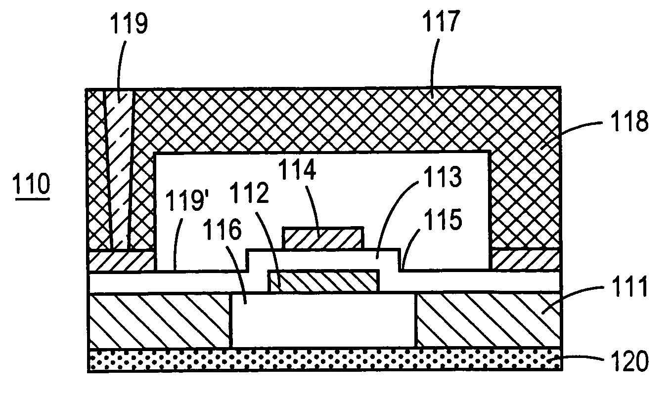
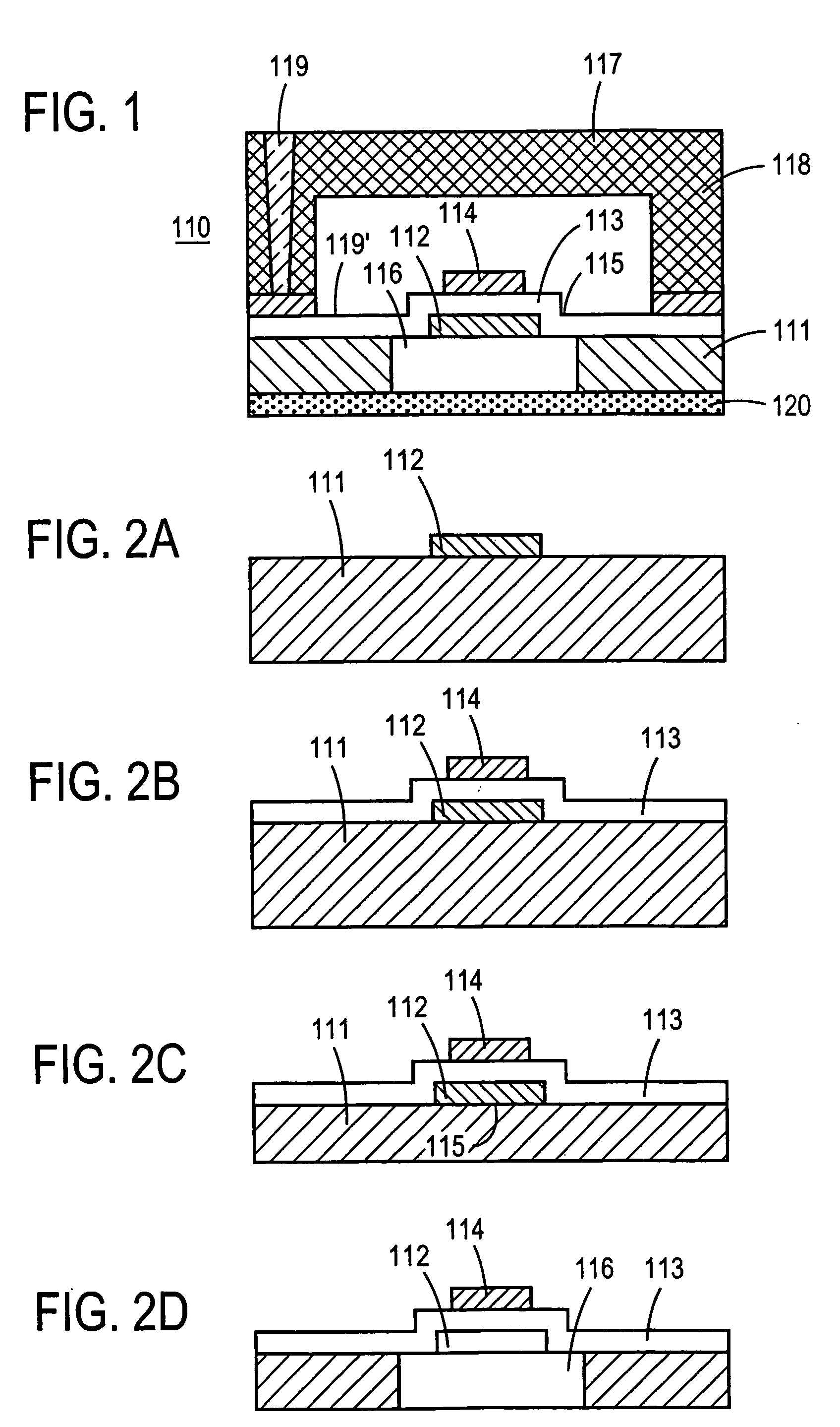
[0023] As shown in FIG. 1, an exemplary embodiment of the present invention is illustrated by a resonator 110, which includes a support structure 111. The support structure 111 can be made of any material that provides a rigid anchor to a resonator membrane 115 (described below) so at to not adversely interfere with membrane vibration. While it can be of nearly any material capable of physical support of the membrane 115 because the support structure 111 is not necessarily otherwise related to the performance of the resonator, it is commonly a Silicon (Si) or Gallium Arsenide (GaAs) wafer so as to permit the formation of other circuit elements on the same wafer to form an integrated monolithic device and / or to utilize conventional and even common semiconductor processing techniques for producing CMOS and bipolar devices, for instance. As a non-exclusive list, other materials include quartz, sapphire or magnesium oxide, and even somewhat flexible plastics, polymers and the like.

[002...

second embodiment

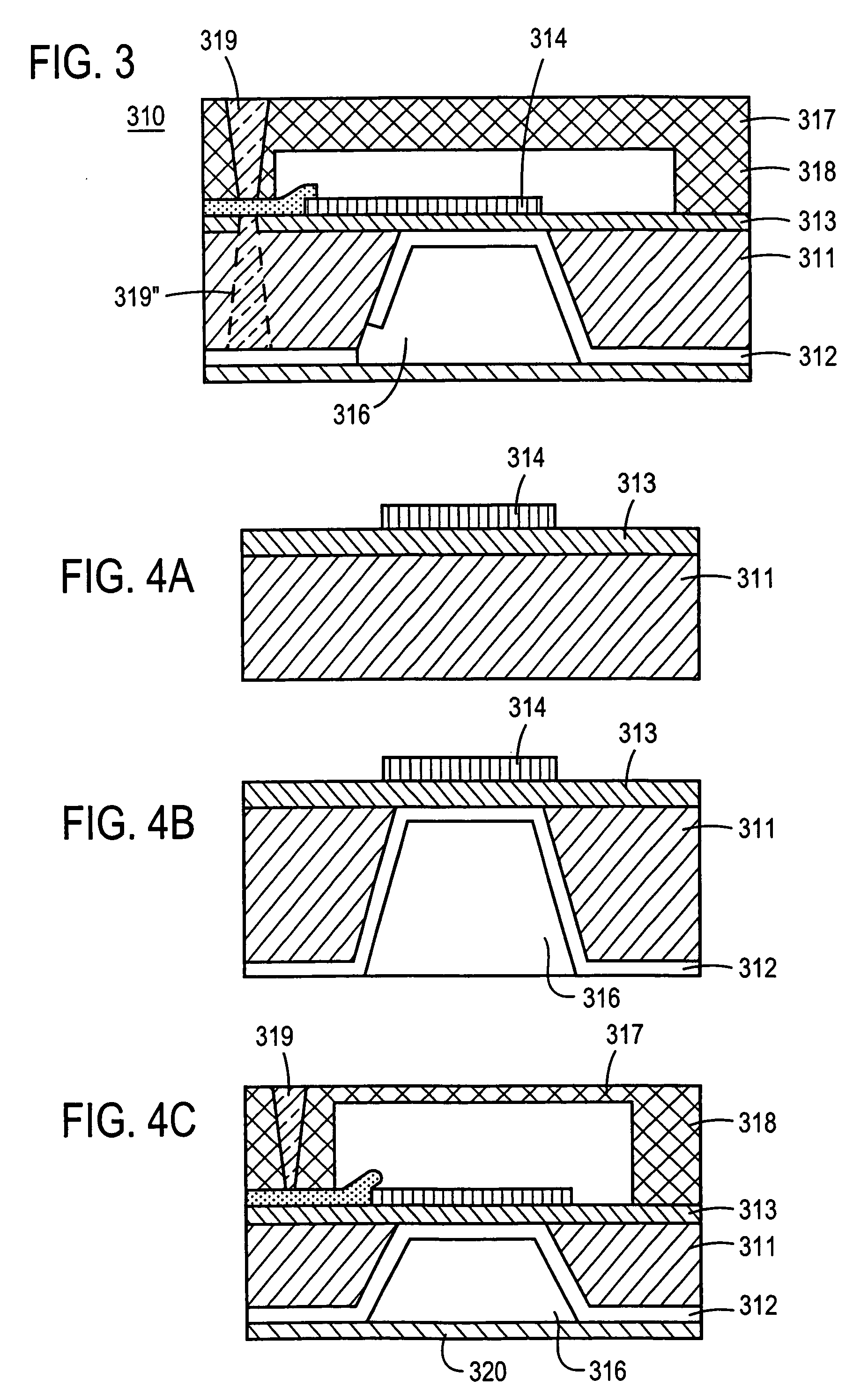
[0038] Another embodiment of a resonator 310 is illustrated in FIG. 3, wherein the first electrode 312 extends from a surface of the piezoelectric layer 313 adjacent to the first surface of the support structure 311, across at least part of a wall of the cavity 316 and onto the second surface of the support structure 311. This embodiment facilitates back surface electrical connections and can be used to avoid step edges or discontinuities in the piezoelectric layer 313 of the membrane structure 315 that might otherwise cause a loss in lateral mode energy.

[0039] The method of manufacturing the second embodiment of the resonator as illustrated in FIG. 3 is similar to but not identical to the method used in the manufacturing of the embodiment shown in FIG. 1. Specifically, the manufacturing a resonator 310 in accordance with the embodiment shown in FIG. 4A includes the steps of patterning a piezoelectric layer 313 on a support structure 311 and patterning a second electrode 314 on the...

third embodiment

[0043]FIG. 5 shows a resonator 510 according to a third embodiment that includes a support structure 511 and a first electrode 512 located adjacent to a first surface of the support structure 511. A piezoelectric layer 513 is located adjacent to the first electrode 512 and the first surface of the support structure 511. A second electrode 514 is located adjacent to the piezoelectric layer 513 on a side of the piezoelectric layer 513 opposite to and in electrical isolation from the first electrode 512. The first electrode 512, the piezoelectric layer 513 and the second electrode 514 collectively form a resonant membrane structure 515.

[0044] The support structure 511 includes a cavity 516 that extends under the first electrode 512 such that at least part of the membrane structure 515 is over the cavity 516. The support structure 511 also includes the via hole 516A extending from the cavity 516 to a second surface of the support structure 511 opposite to the first surface of the suppo...


PUM

PropertyMeasurementUnit
angleaaaaaaaaaa
thicknessaaaaaaaaaa
thicknessaaaaaaaaaa

Abstract

A resonator having a membrane formed of a piezoelectric layer sandwiched between first and second electrode is suspended above a cavity formed from the back surface of the support structure. In one embodiment, the cavity walls are substantially perpendicular to the back surface. In another embodiment, the first electrode is formed in the cavity such that it is electrically connected to an electrode on the back surface of the support structure. In yet another embodiment, the cavity is formed via an etch through via holes in the back surface of the support structure, which leads to greater flexibility in designing a method of manufacture while reducing the need for alignment relative to other designs.

Description

FIELD OF THE INVENTION [0001] The present invention relates to a bulk mode piezoelectric vibrator, such as used in an electrical filter and / or duplexer, for instance, and to methods of making same. BACKGROUND OF THE INVENTION [0002] Acoustic resonators are used in many applications that require a precisely controlled frequency, including but not limited to wireless devices such as mobile telephones, pagers, radio receivers, microwave satellite communication devices, and various types of handheld electronics. In these devices, it is often important for components to take up as little space as possible on a monolithic integrated circuit, for instance, particularly if the resonator is part of a monolithic integrated circuit. [0003] Acoustic resonators are useful in many applications such as electronic filters. Filters that use piezoelectric materials are particularly useful for frequencies above about 300 MHz where a thin film, non-conductive piezoelectric resonator is commonly used. P...

Claims


Application Information

Patent Timeline
Patent Type & Authority Applications(United States)
IPC IPC(8): H03H9/17H03H3/02H03H9/02H03H9/58H03H9/70
CPCH03H3/02H03H9/02149H03H9/105Y10T29/42H03H9/174H03H2003/021H03H2003/023H03H9/173B65B51/146B65B65/02H05B3/20
Inventor SONG, IN-SANGHA, BYEOUNG-JUKIM, DUCK-HWANPARK, YUN-KWON
Owner SAMSUNG ELECTRONICS CO LTD
Why Eureka
Try Eureka