Planarized and silicided trench contact

a trench contact and silicide technology, applied in the field of planarized and silicided, can solve the problems of only metalizing the gate bus region, destroying the entire device, and undesirable trade-off between fast switching speed, and achieve the effect of maximizing device density and facilitating gate conta

Inactive Publication Date: 2004-09-23
ADVANCED ANALOGIC TECHNOLOGIES INCORPORATED +1
View PDF13 Cites 38 Cited by
  • Summary
  • Abstract
  • Description
  • Claims
  • Application Information

AI Technical Summary

Benefits of technology

[0029] A trench-gated vertical power MOSFET and fabrication processes for such power MOSFETs use a continuous conductive gate structure within trenches to avoid problems that topology causes when a gate bus extends above a substrate surface. The conductive gate structure forms gates in device trenches in an active device region of the power MOSFET and forms a gate bus in a gate bus trench. The gate bus trench that connects to the device trenches can be wide to facilitate forming a gate contact to the gate bus, while the device trenches are narrow to maximize device density. CMP processes can be used to planarize the conductive gate structure and / or overlying insulating layers, and the processes are compatible with processes forming self-aligned or conventional contacts in the active device region.
[0031] Power MOSFETs in accordance with alternative embodiments of the invention can employ a variety of contact structures. Conventional non-self-aligned gate and source contacts can be formed through a planarized insulating layer to the gate bus in the second trench and source regions in the substrate. The planar topology provided by CMP processes that the in-trench gate structure allows facilitates accurate etching of contact openings.
[0032] In an architecture having self-aligned source contacts, an insulating material residing in the trenches above the gate structure, has a top surface of the insulating material that is coplanar with the top surface of the substrate. A metal contact layer formed on the planar surface of the substrate and the insulating material includes a source contact region that contacts the source region of the vertical device formed in the substrate's mesa. The insulating material in the trenches prevents the source contact region from shorting to the gate structure. A gate contact region of the metal layer contacts the gate bus through an opening formed through the insulating material in the gate bus trench.
[0035] Another specific embodiment of the invention is a fabrication process for a power MOSFET. Generally, the fabrication process includes device and gate bus trenches in a substrate, which may include an epitaxial layer. A conductive gate structure is then formed that extends continuously from the device trenches into the gate bus trench. Doping of a mesa in the substrate adjacent to a device trench forms a vertical device including a source region, a channel region, and a drain region that are vertically aligned along a wall of the device trench. The process creates a structure including the conductive gate structure in the trenches and permits a chemical mechanical polishing (CMP) of the structure. Thus, formation of a contact layer is after the CMP process, which improves the reliability of the source contact to the vertical devices and the gate contact to the gate structure in the gate bus trench. The gate bus trench is generally shallower and wider than the device trenches.

Problems solved by technology

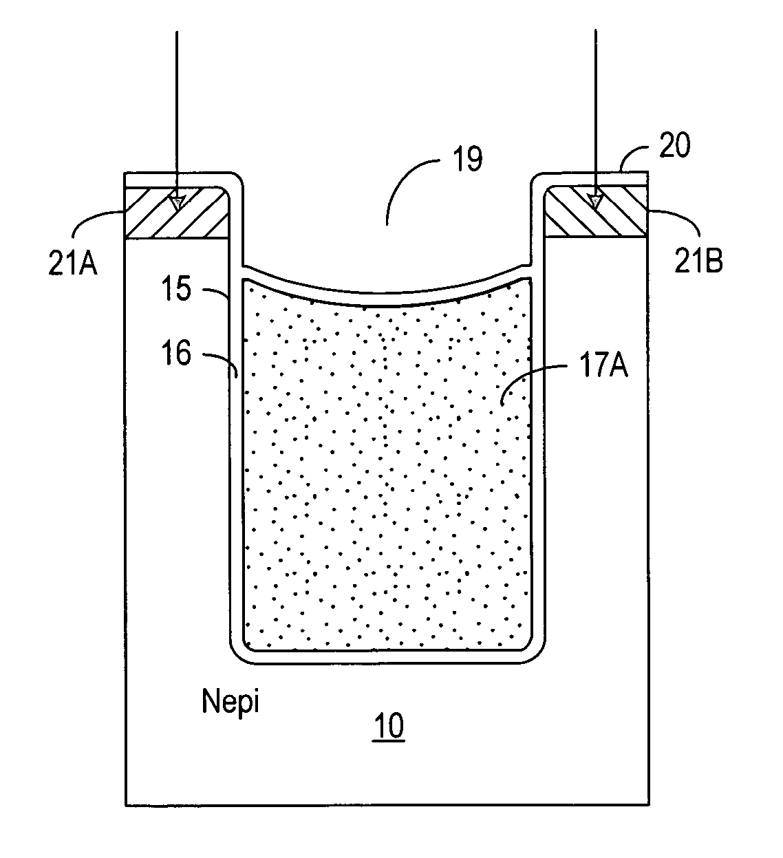
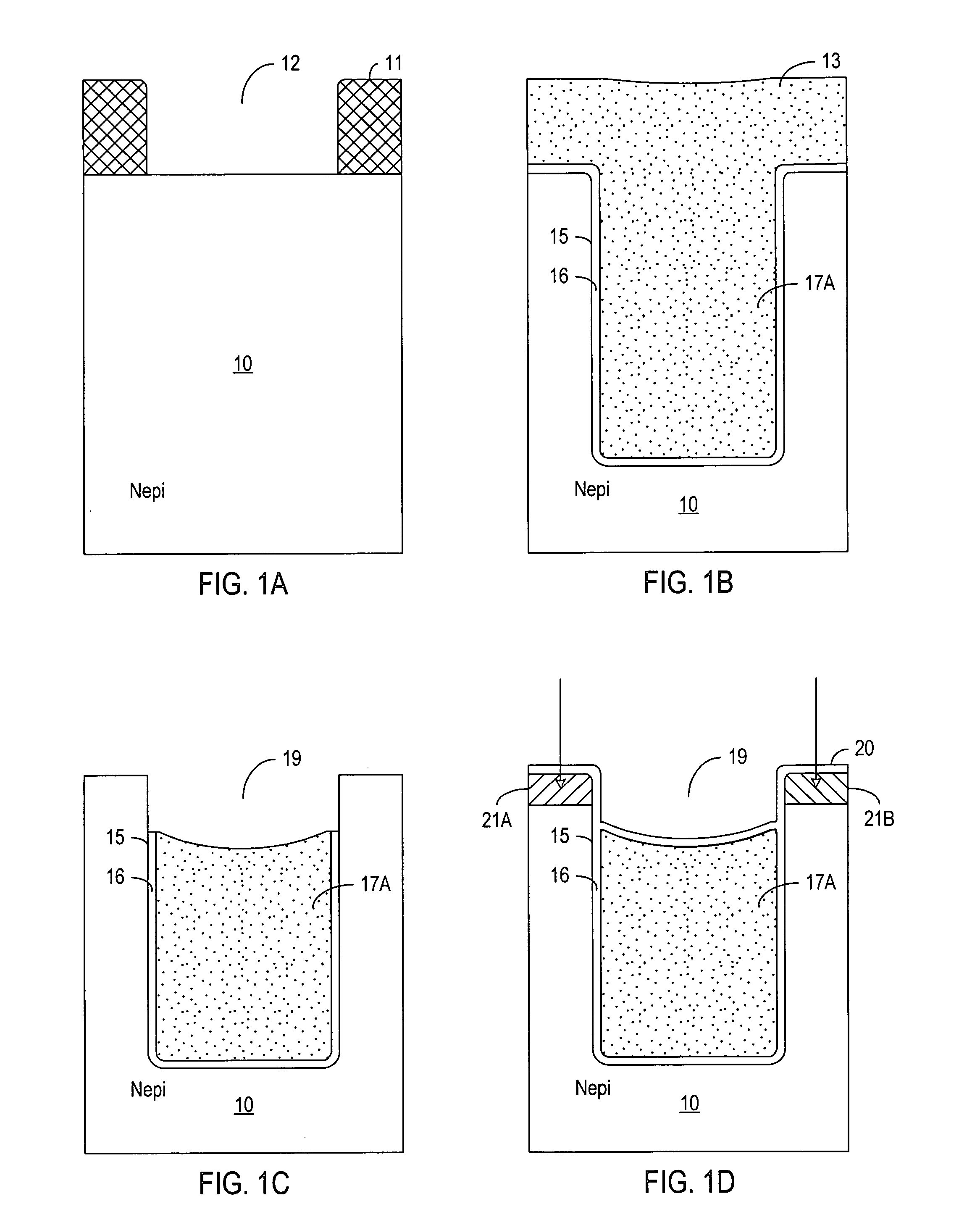
One complexity in the fabrication involves etching the trench, oxidizing it with a high quality oxide and filling the trench with a highly doped layer of polysilicon.
Another challenge during wafer fabrication involves the steps of etching this gate polysilicon down into the trench and sealing it with an insulator so that it doesn't electrically short to a thick layer of source metal, said metal being formed subsequent to the trench gate and covering much of the wafer's surface.
If any one cell out of millions of cells comprising a single device becomes shorted, the entire device is ruined.
But, since most vertical power devices employ a single layer metal process (the metal generally being several microns thick), such gate bus regions can only be metalized by interrupting the source metal.
The need for a metalized gate bus therefore conflicts with the need for uninterrupted top source metal, forcing an undesirable tradeoff between fast switching speeds and the lowest possible resistance device.
A difficulty with manufacturing MOSFET 50 of FIG. 2A is the non-planar topography present during critical photolithography and planarization operations.
Extreme topography can create problems during photomasking, during etching, and during planarization operations, and virtually precludes the use of chemical mechanical polishing (CMP) techniques.
Large step heights may also lead to step coverage problems for depositions and conformal coatings.
Other complications in trench MOSFET manufacturing may occur at any number of steps in the fabrication sequence, and may later exacerbate issues with trench filling, planarization, and topography.
The misshaped trenches become very difficult to planarize using polysilicon overfill and etch-back methods since the trench opening is wider than the other trenches within the device.
As shown in the drawing of FIG. 2D, several problem areas may occur in such a device.
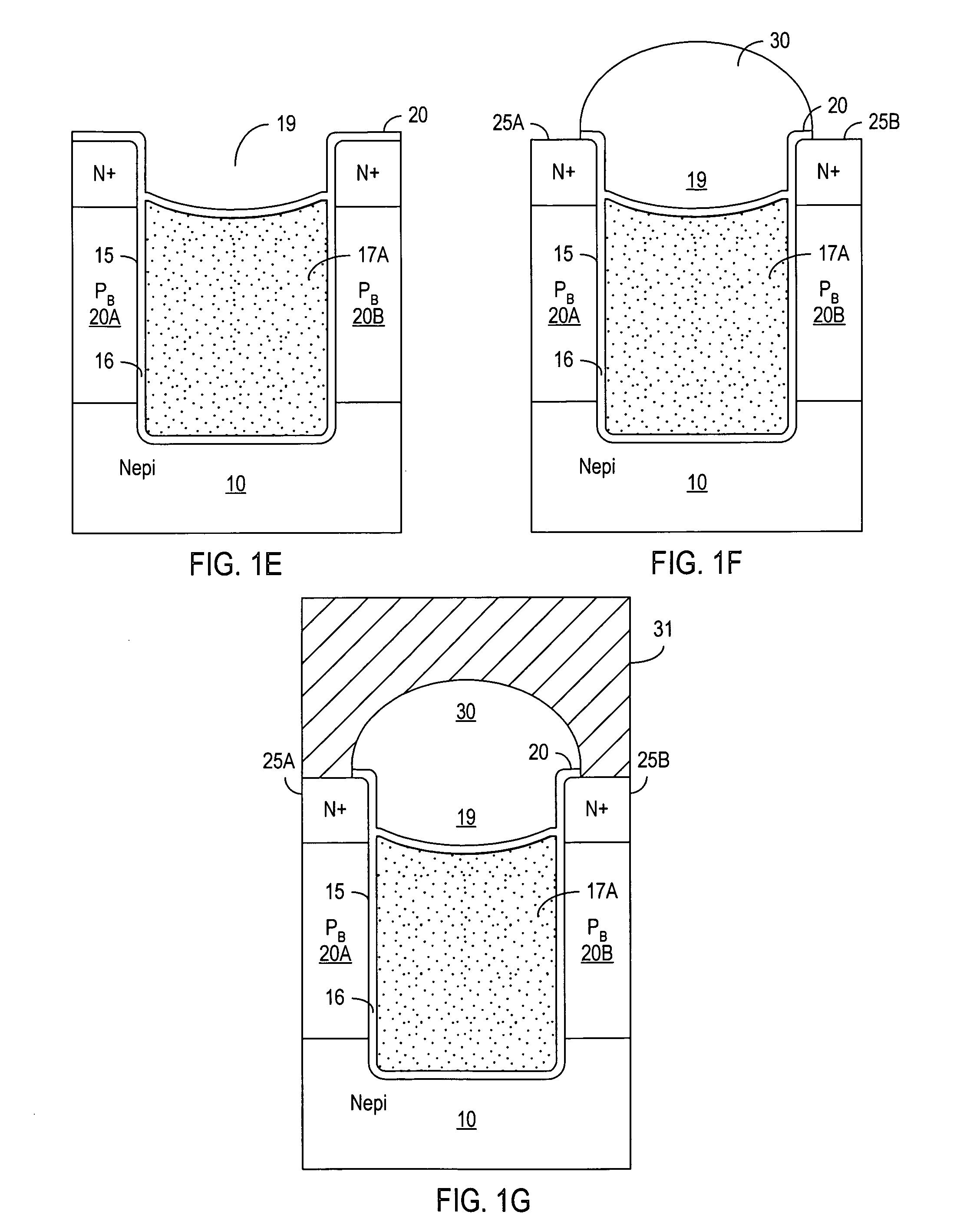
Furthermore, polysilicon gate 83 must vertically overlap the bottom of N+ source 86 in region 102 or the MOSFET will not operate properly (causing high on-resistance and possible loss of functionality).
In each case shown, poor planarization leads to defects, poor uniformity, and yield loss.
If thickness x is minimized to prevent step height related step coverage problems later, the depth of the surface depressions 135A, 135B, and 135C at the top of the active polysilicon trench gates will be extreme and may be difficult to fill later.
Thick polysilicon, e.g., over 1 to 1.5 .mu.m thick, requires long processing time, adversely adding to wafer costs.
Either location may later cause problems with glass depositions, TiN metallization, or metal breakage.
Such topography prevents the use of chemical mechanical polishing (CMP) techniques, since mechanical planarization of the trench polysilicon would remove the gate bus entirely from the device's surface.
Uniformity across a die and across a wafer can therefore be problematic in achieving highly manufacturable products.
All these failures may compromise the performance, yield, or reliability of a trench MOSFET.
The problems are greatly exaggerated by the non-planar surface of the device, requiring photolithographic-masking, etching, etch backs, planarization, and depositions to behave similarly (or identically) on different heights within a single device.
Not only does the extreme topography of today's vertical trench power MOSFET processes limit the device's cell density and performance, its high intrinsic gate resistance limits its switching speed, mandating the need for additional metalized gate bus regions.
. . +.sub.rgm) can suffer serious gate propagation delays, even switching ten times slower than cells near the metalized gate bus.
During slow transients, the simultaneous presence of both voltage across the device and current through the device greatly increases power losses in the device and lowers the efficiency of using such a switch in many applications.
More gate bussing and less active cells increases the switch's on-resistance or die size, and therefore cost.
Moreover the gate bus regions exacerbate the non-planar topography issues that further limit device density and performance improvements.

Method used


Image

  • Planarized and silicided trench contact
  • Planarized and silicided trench contact
  • Planarized and silicided trench contact

Examples


Embodiment Construction

[0066] As shown in FIG. 9A, a trench-gated vertical power MOSFET (also known as a trench DMOS device) associated with this invention comprises an array of tightly packed devices in an array of stripes or polygonal cells (the portion located beneath metal 407A in the drawing) having a series of trenches 403A, 403B, 403C etched into the silicon surface, lined with a thin gate oxide 399A, 399B, 399C in all (or along some portion) of the trenches, and filled with a conductor such as heavily-doped polysilicon 404A, 404B, 404C. The embedded polysilicon is not contacted within this "active cell array", but instead is contacted by extending the trench with its embedded polysilicon into another region to contact the trench polysilicon with metal. Between trenches lies a mesa region typically used to integrate the MOSFET's source, body (channel), and body contact features. Within the active array, the mesa region includes contact windows 408A, 408B, 408C, and 408D to facilitate electrical con...


PUM


Abstract

Power MOSFETs and fabrication processes for power MOSFETs use a continuous conductive gate structure within trenches to avoid problems arising from device topology caused when a gate bus extends above a substrate surface. The gate bus trench and / or gate structures in the device trenches can contain a metal / silicide to reduce resistance, where polysilicon layers surround the metal / silicide to prevent metal atoms from penetrating the gate oxide in the device trenches. CMP process can remove excess polysilicon and metal and planarize the conductive gate structure and / or overlying insulating layers. The processes are compatible with processes forming self-aligned or conventional contacts in the active device region.

Description

CROSS-REFERENCE TO RELATED PATENT APPLICATION[0001] This is a divisional and claims the priority of U.S. patent application Ser. No. 10 / 383,231, filed on Mar. 5, 2003.[0002] The fabrication of trench-gated devices is common to many high performance power semiconductor devices today. Such devices include the trench-gated vertical power MOSFET (a.k.a. trench DMOS, trench FET, UMOS, etc.) and its many variants and derivatives, relying on vertical current flow through a semiconductor from a topside metal contact to a metalized backside contact whereby the potential on a trench-embedded gate electrode controls the current in said device. Such embedded trench gates actually include the gate electrode of a MOSFET whose channel is electrically induced on the sidewall of an etched silicon trench perpendicular to the wafers surface. Devices employing a trench-gated vertical channel differ dramatically from conventional MOSFETs whose gate is located above and parallel to the wafer's surface (r...

Claims


Application Information

Patent Timeline
Patent Type & Authority Applications(United States)
IPC IPC(8): H01L21/336H01L29/423H01L29/45H01L29/49H01L29/78
CPCH01L29/1095H01L29/4236H01L29/42368H01L29/456H01L29/7813H01L29/4933H01L29/4941H01L29/66734H01L29/4925H01L29/7811H01L29/42372
Inventor WILLIAMS, RICHARD K.CORNELL, MICHAEL E.CHAN, WAI TIEN
Owner ADVANCED ANALOGIC TECHNOLOGIES INCORPORATED
Why Eureka
Try Eureka