Light-emitting devices having multiple encapsulation layers with at least one of the encapsulation layers including nanoparticles and methods of forming the same

a technology of light-emitting devices and nanoparticles, which is applied in the field of microelectronic devices, can solve the problems of epoxy-based encapsulation layers that may optically degrad

Active Publication Date: 2005-10-13
CREELED INC
View PDF27 Cites 150 Cited by
  • Summary
  • Abstract
  • Description
  • Claims
  • Application Information

AI Technical Summary

Benefits of technology

[0008] In still other embodiments of the present invention, the at least one physical property comprises index of refraction, thermal conductivity, mechanical strength, abrasion resistance, and / or optical stability.
[0013] In still further embodiments of the present invention, the at least one physical property of the second encapsulation layer comprises index of refraction, thermal conductivity, mechanical strength, abrasion resistance, and / or optical stability.

Problems solved by technology

Unfortunately, an epoxy-based encapsulation layer may optically degrade when used with relatively short wavelength (e.g., 525 nm), high flux LEDs.

Method used


Image

  • Light-emitting devices having multiple encapsulation layers with at least one of the encapsulation layers including nanoparticles and methods of forming the same
  • Light-emitting devices having multiple encapsulation layers with at least one of the encapsulation layers including nanoparticles and methods of forming the same
  • Light-emitting devices having multiple encapsulation layers with at least one of the encapsulation layers including nanoparticles and methods of forming the same

Examples


Embodiment Construction

[0020] While the invention is susceptible to various modifications and alternative forms, specific embodiments thereof are shown by way of example in the drawings and will herein be described in detail. It should be understood, however, that there is no intent to limit the invention to the particular forms disclosed, but on the contrary, the invention is to cover all modifications, equivalents, and alternatives falling within the spirit and scope of the invention as defined by the claims. Like numbers refer to like elements throughout the description of the figures. In the figures, the dimensions of layers and regions are exaggerated for clarity. Each embodiment described herein also includes its complementary conductivity type embodiment.

[0021] It will be understood that when an element such as a layer, region or substrate is referred to as being “on” another element, it can be directly on the other element or intervening elements may also be present. It will be understood that if...


PUM


Abstract

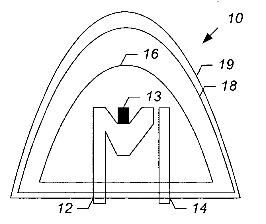
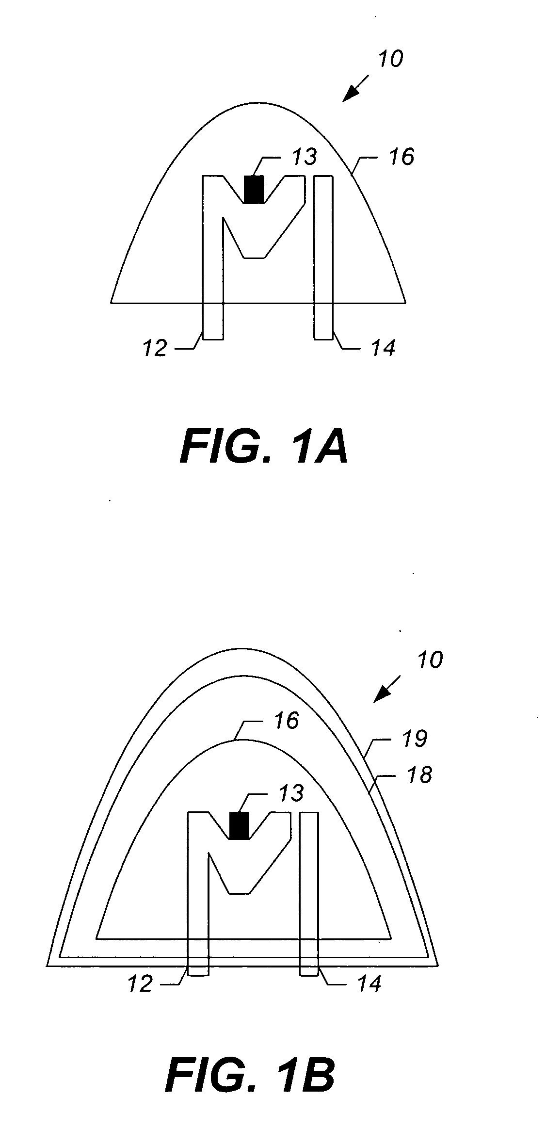
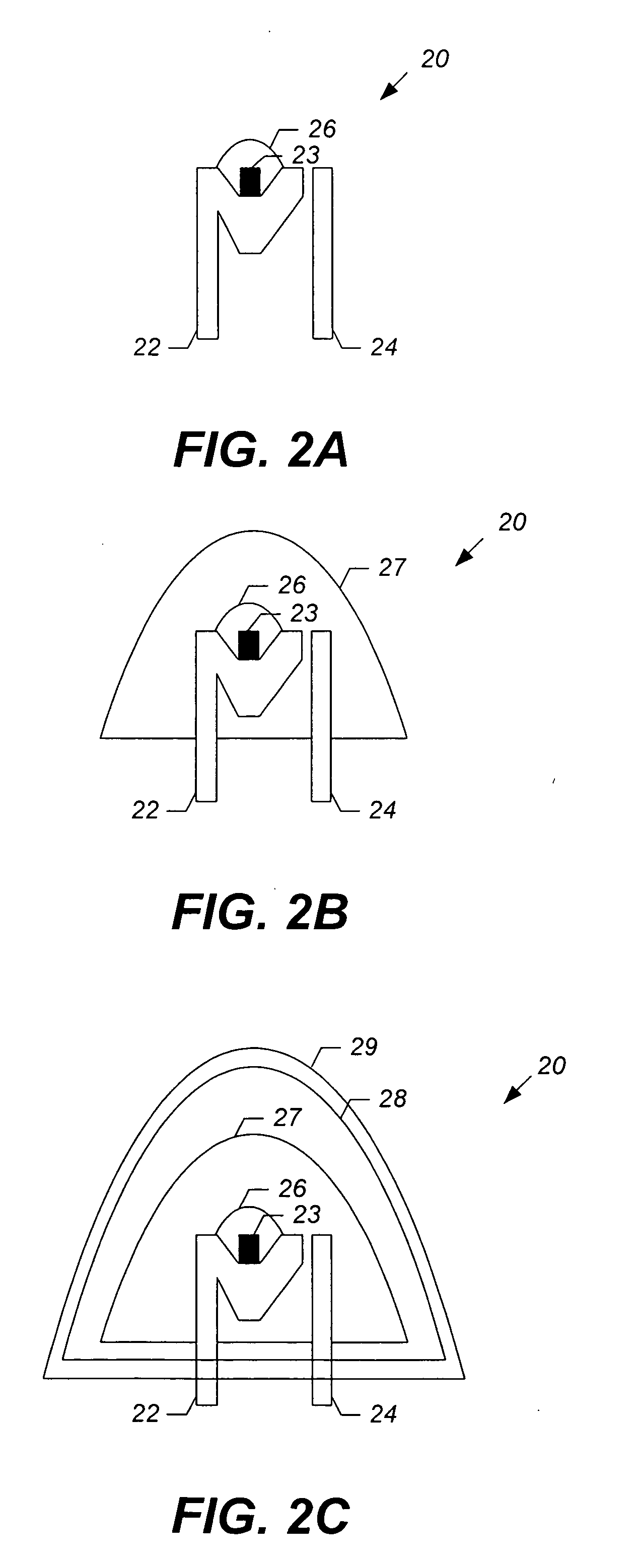
A light-emitting device includes an active region that is configured to emit light responsive to a voltage applied thereto. A first encapsulation layer at least partially encapsulates the active region and includes a matrix material and nanoparticles, which modify at least one physical property of the first encapsulation layer. A second encapsulation layer at least partially encapsulates the first encapsulation layer.

Description

FIELD OF THE INVENTION [0001] The present invention relates generally to microelectronic devices and fabrication methods therefor, and, more particularly, to light-emitting devices and fabrication methods therefor. BACKGROUND OF THE INVENTION [0002] Light-emitting diodes (LEDs) are widely used in consumer and commercial applications. As is well known to those skilled in the art, a light-emitting diode generally includes an active region on a microelectronic substrate. The microelectronic substrate may comprise, for example, gallium arsenide, gallium phosphide, alloys thereof, silicon carbide, and / or sapphire. Continued developments in LEDs have resulted in highly efficient and mechanically robust light sources that can cover the visible spectrum and beyond. These attributes, coupled with the potentially long service life of solid state devices, may enable a variety of new display applications, and may place LEDs in a position to compete with well entrenched incandescent and / or fluor...

Claims


Application Information

Patent Timeline
Patent Type & Authority Applications(United States)
IPC IPC(8): H01L33/50H01L33/52H01L33/56H05B33/04
CPCH01L33/52H01L33/56H05B33/04H01L33/54
Inventor NEGLEY, GERALD H.TARSA, ERIC
Owner CREELED INC
Why Eureka
Try Eureka