Semiconductor memory device and manufacturing method thereof

Inactive Publication Date: 2005-10-13
MONTEREY RES LLC
View PDF1 Cites 61 Cited by
  • Summary
  • Abstract
  • Description
  • Claims
  • Application Information

AI Technical Summary

Problems solved by technology

The flash memory using a floating gate prevails among them, however, it is difficult for the memory of this type to allow a tunnel insulating film to be thinner, which is an obstacle for the mass storage.
Accordingly, in order to form the ON film or the ONO film by the CVD method, there exists a problem that the high temperature heat treatment for a long time is fundamental and that a matching property is extremely low with respect to the miniaturization of a semiconductor element, especially a transistor, of a peripheral circuit region of a memory cell.
If the bit line is formed after the ON film or the ONO film is formed to avoid the diffusion, there is a problem that damage is generated in the ON film or the ONO film and the decrease of a withstand voltage is caused.
However, the formation of the CVD nitride film requires the high temperature as described above, and further, in the case of the highly integrated MNOS structur

Method used


Image

  • Semiconductor memory device and manufacturing method thereof
  • Semiconductor memory device and manufacturing method thereof
  • Semiconductor memory device and manufacturing method thereof

Examples


specific embodiments

[0043] Based on the aforementioned basic gist of the present invention, specific embodiments will be described below.

first embodiment

[0044] In the present invention, an embedded bit line type SONOS transistor as a semiconductor memory device will be disclosed. For convenience, a structure of the transistor will be explained with a manufacturing method thereof.

[0045] In the semiconductor memory device, a SONOS transistor in a memory cell array region is a planar type and a CMOS transistor is formed in a peripheral circuit.

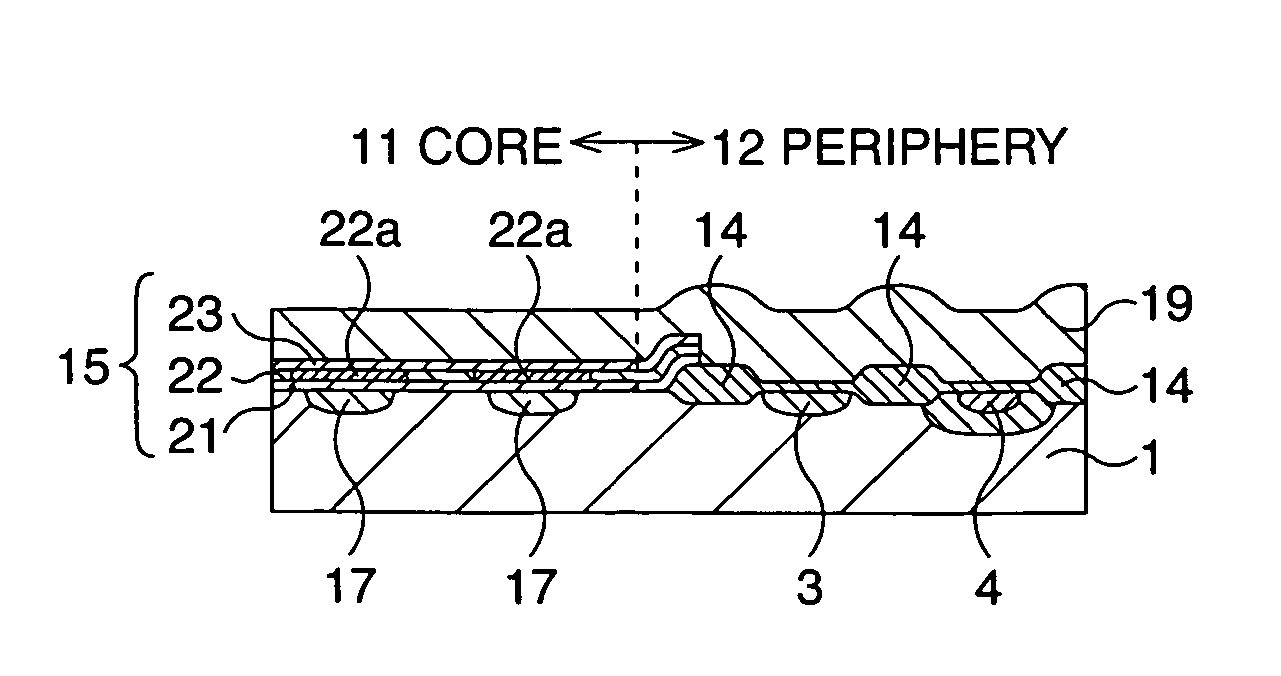
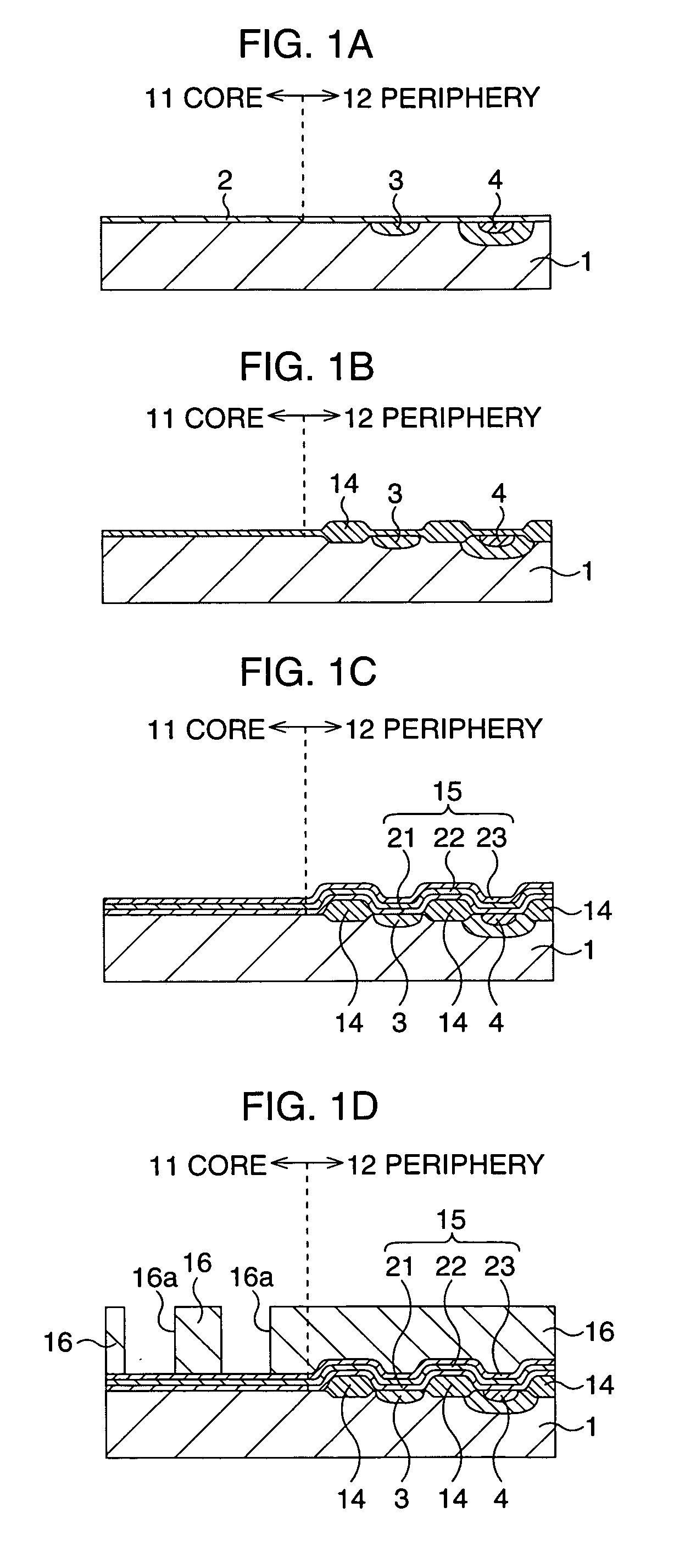
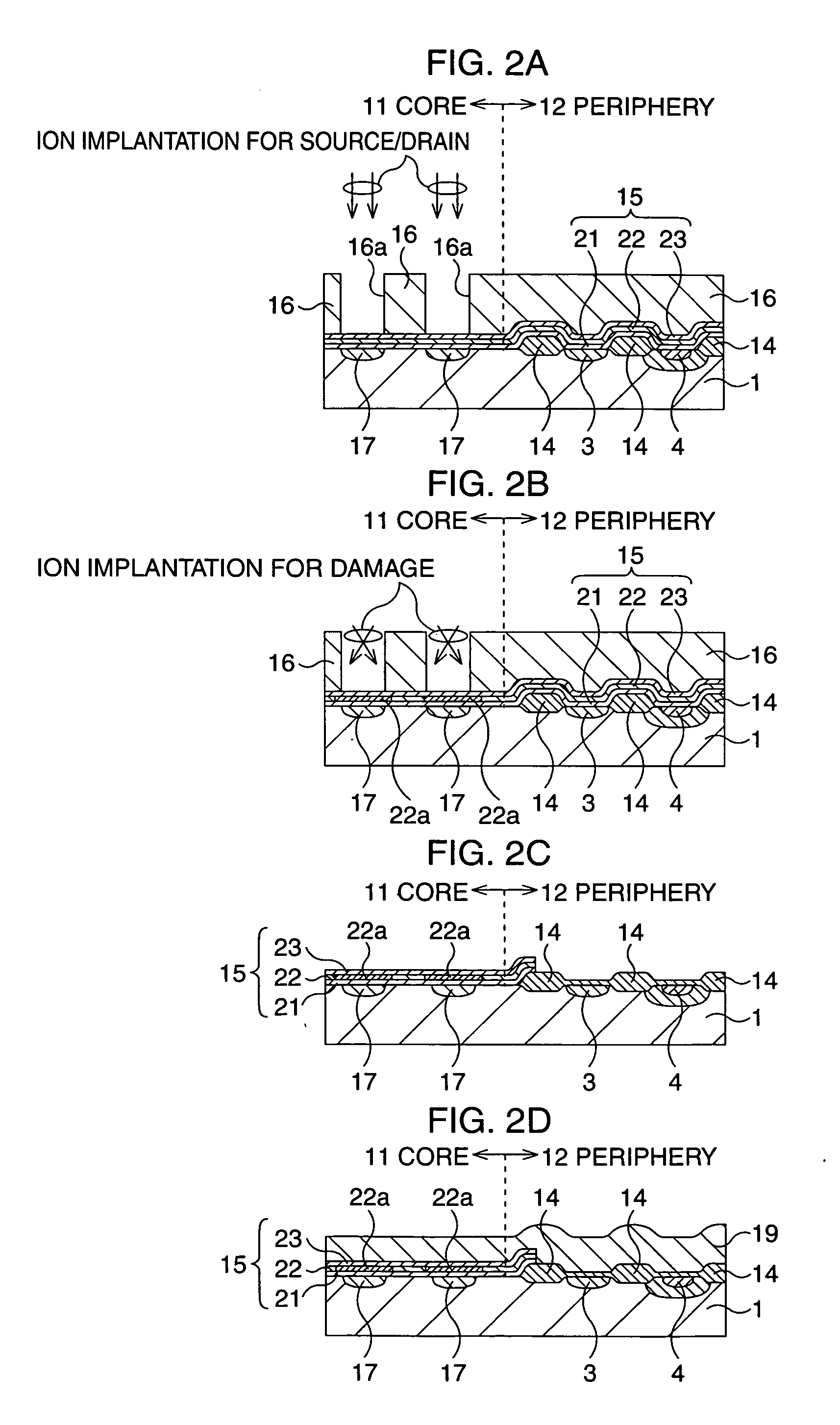
[0046]FIG. 1A to FIG. 1D and FIG. 2A to FIG. 2D are schematic sectional views showing a manufacturing method of the semiconductor memory device including an embedded bit line type SONOS transistor according to the present invention in order of process, and FIG. 3B is a schematic plan view corresponding to FIG. 3A. In FIG. 3A and FIG. 3B, the memory cell array region (core region) alone is shown, a cross section taken along the line I-I of FIG. 3B corresponds to a core X of FIG. 3A, and a cross section taken along the line II-II corresponds to a core Y of FIG. 3A respectively.

[0047] First, as s...

modification example

[0073] Here, some modification examples of the present embodiment are explained. In these modification examples, a semiconductor memory device including a embedded bit line type SONOS transistor are illustrated in the same way as the present embodiment, however, these examples differ from the present embodiment in a part of the main process.


PUM


Abstract

After an ONO film in which a silicon nitride film (22) formed by a plasma nitriding method using a plasma processor having a radial line slot antenna is sandwiched by silicon oxide films (21), (23), a bit line diffusion layer (17) is formed in a memory cell array region (11) by an ion implantation as a resist pattern (16) taken as a mask, then lattice defects are given to the silicon nitride film (22) by a further ion implantation. Accordingly, a highly reliable semiconductor memory device can be realized, in which a high quality nitride film is formed in a low temperature condition, in addition, the nitride film can be used as a charge trap film having a charge capture function sufficiently adaptable for a miniaturization and a high integration which are recent demands.

Description

TECHNICAL FIELD [0001] The present invention relates to a semiconductor memory device and a manufacturing method thereof, which has a gate insulating film including a nitride film and capable of holding information by storing the charge in the nitride film. BACKGROUND ART [0002] In recent years, a multitude of so-called flash memories are used as a rewritable semiconductor memory device. The flash memory using a floating gate prevails among them, however, it is difficult for the memory of this type to allow a tunnel insulating film to be thinner, which is an obstacle for the mass storage. Hence, a multi-value memory cell is thought out, in which a threshold value of a transistor is varied by controlling a charge amount to the floating gate when writing, and multi-value data is allowed to be stored in one memory cell. [0003] A new multi-value memory cell having an MNOS structure or a SONOS structure, different from the floating gate type memory cell, is proposed, which applies, to th...

Claims


Application Information

Patent Timeline
IPC IPC(8): H01L21/28H01L21/8247H01L21/3115H01L21/318H01L21/336H01L21/8246H01L27/105H01L27/115H01L29/788H01L29/792
CPCH01L21/28282H01L21/31155H01L21/3185H01L27/105H01L21/02252H01L27/11573H01L29/66833H01L21/022H01L21/0217H01L27/11568H01L29/40117H10B43/30H10B43/40
Inventor HIGASHI, MASAHIKONAKAMURA, MANABUSERA, KENTARONANSEI, HIROYUKIUTSUNO, YUKIHIROTAKAGI, HIDEOKAJITA, TATSUYA
Owner MONTEREY RES LLC
Why Eureka
Try Eureka