Circuit device

Inactive Publication Date: 2005-10-13
SANYO ELECTRIC CO LTD
View PDF12 Cites 9 Cited by
  • Summary
  • Abstract
  • Description
  • Claims
  • Application Information

AI Technical Summary

Benefits of technology

[0022] Second, by fixing the bonding wire directly to the passive element, electrical connection to other constituent components is realized. Thus, a part of the conductive pattern can be disposed below the bonding wire. In a conventional case, since the passive element is connected to the other constituent components by use of the conductive pattern, if the conductive pattern intersects with the conductive pattern connected to the passive element, it is required to form a two-layered wiring structure. Meanwhile, according to an embodiment of the present invention, the conductive patterns can intersect with each other in a single layer structure. Thus, a packaging density can be improved.
[0023] Third, the passive element can be bonded on the semiconductor element. Thus, the mounting area can be reduced, and high-frequency characteristics can be improved by shortening the bonding wires connected to the semiconductor element.
[0025] Fifth, since fixing can be performed without using a solder material, occurrence of cracks in the solder material due to stress on a resin package can be prevented. Thus, reliability is improved.
[0026] Sixth, since a fillet made of the solder material is not formed on the side of the passive element, an area for mounting the passive element can be reduced. Thus, the packaging density of the entire device can be improved.

Problems solved by technology

Specifically, there are problems that, for the connection of the passive element, the multi-layered structure has to be formed by increasing costs and the number of production process, or the mounting area has to be further increased.
Furthermore, in the case of fixing by use of the solder material, a device having a structure subjected to resin sealing has the following problems.
This is because, if the reflow temperature reaches the melting point of solder or more, solder is remelted to cause short circuit or package destruction.
In this case, if the package is distorted by heat generated after resin sealing, crack occurs in solder or Ag paste.
Thus, reliability is deteriorated.
Moreover, a circuit device using lead-free solder mainly made of tin as fixing means has another problem.
However, mounting by use of high melting point solder also leads to a problem such as destruction of elements.
Accordingly, fixing strength is not perfect.
Specifically, if a passive element in the package is fixed by use of the lead-free solder, and the external terminal (external electrode) is also fixed to the package board by use of the lead-free solder, there arises a problem since the lead-free solder inside is remelted.

Method used


Image

  • Circuit device
  • Circuit device
  • Circuit device

Examples


Embodiment Construction

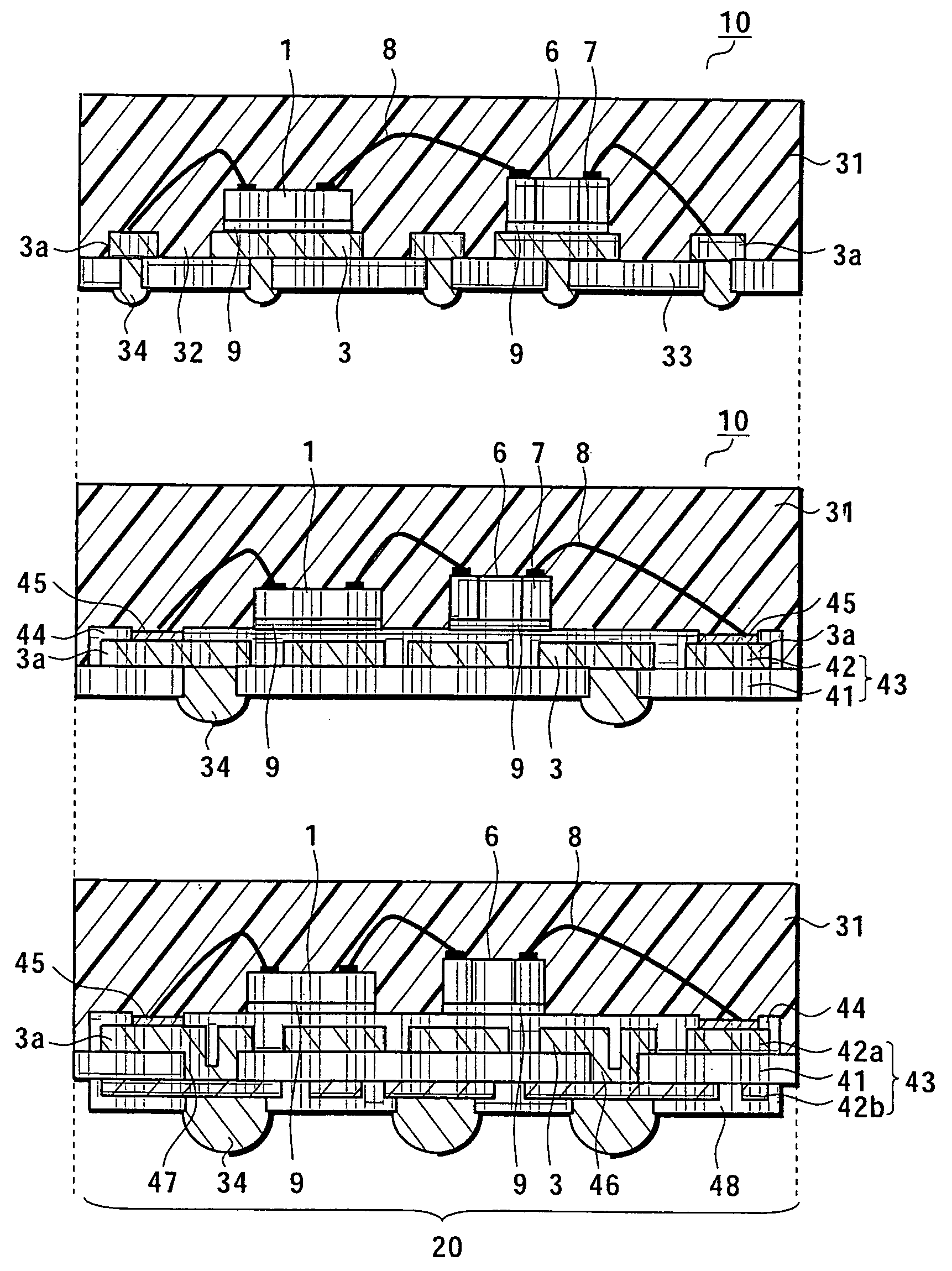
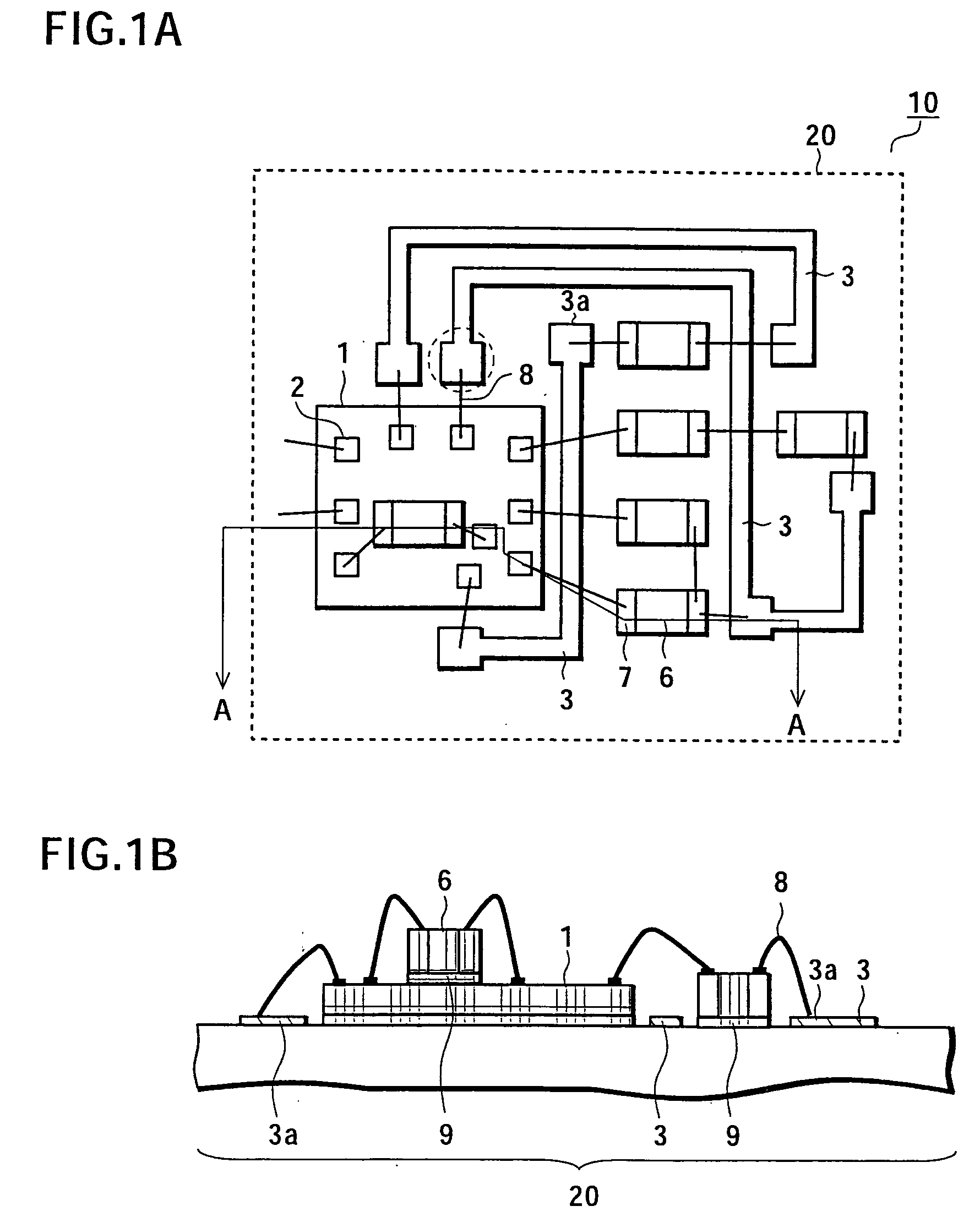
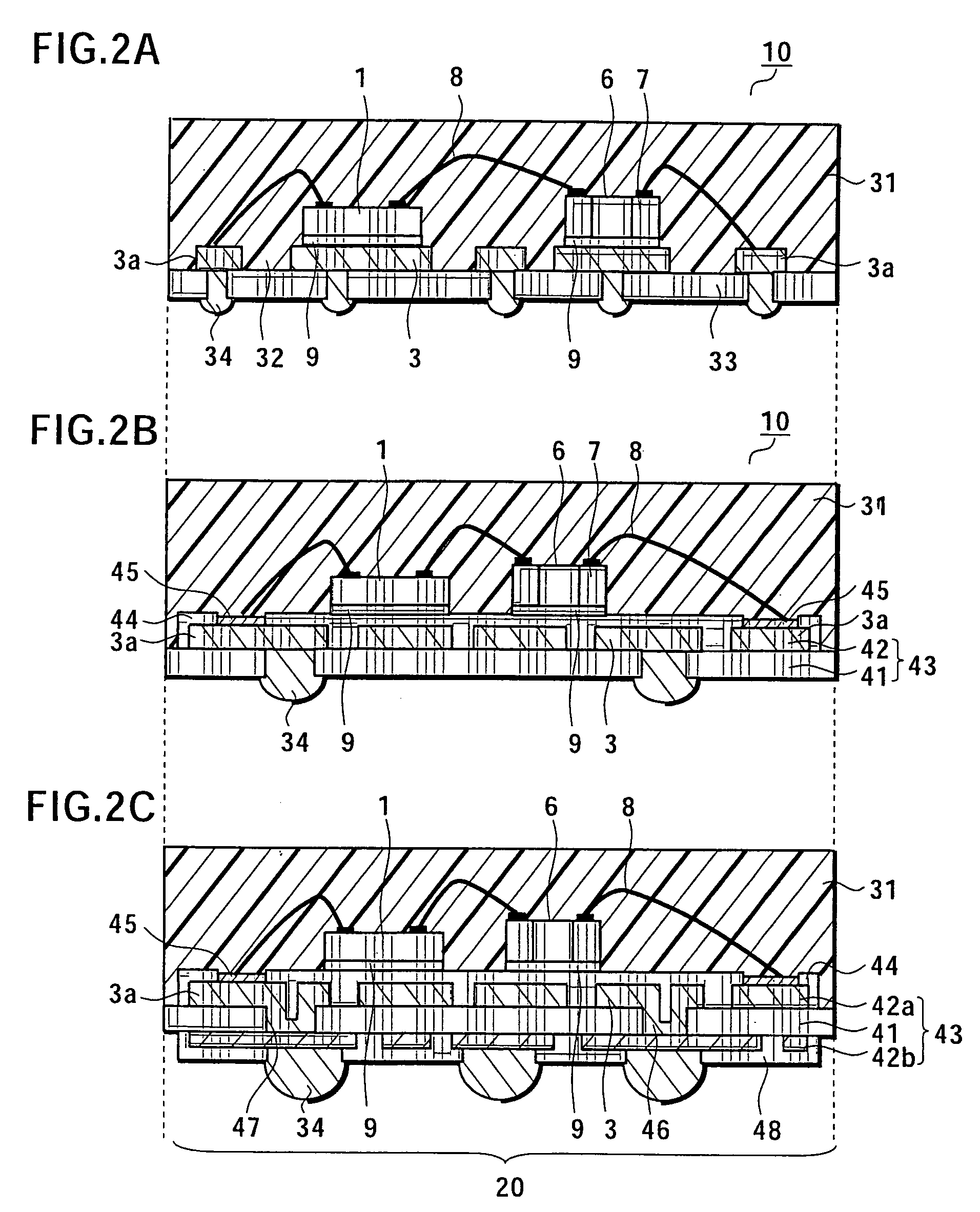
[0035] With reference to FIGS. 1 to 4, an embodiment of a circuit device according to an embodiment of the present invention will be described.

[0036]FIGS. 1A and 1B show the circuit device of this embodiment. FIG. 1A is a plan view, and FIG. 1B is a cross-sectional view along the line A-A in FIG. 1A.

[0037] The circuit device 10 of this embodiment includes a semiconductor element 1, conductive patterns 3, passive elements 6, and bonding wires 8.

[0038] As shown in FIG. 1A, the circuit device has a package region 20 in a predetermined region indicated by the broken line, for example. Note that, in the package region 20 of this embodiment, at least the semiconductor element 1 such as an IC, for example, the conductive patterns 3, and the passive elements 6 are disposed. Here, the package region 20 is one continuous region indicated by the dotted line forming a predetermined circuit. The conductive pattern 3 has a pad part 3a on its end, to which the bonding wire 8 is fixed.

[0039] In...


PUM


Abstract

In the case of mounting a passive element in a circuit device, since an electrode part is tin-plated, the passive element is fixed to a mounting land part by use of a solder material, and wires cannot intersect with each other in a single layer. Accordingly, there are problems such as an increase in a mounting area, a restriction to a reflow temperature in mounting on a printed board, and deterioration of reliability due to solder crack after packaging. The electrode part of the passive element is gold-plated, and a bonding wire is directly fixed to the electrode part. Accordingly, the mounting land part and a pad part for fixing the passive element are reduced, and the wires can intersect with each other even in the single layer. Thus, a packaging density can be improved. Moreover, a restriction that the reflow temperature in mounting the circuit device on the printed board must be set to not more than a melting point of solder can be avoided.

Description

BACKGROUND OF THE INVENTION [0001] 1. Field of the Invention [0002] The present invention relates to a circuit device including a passive element, and more particularly relates to a circuit device having an improved wiring density. [0003] 2. Description of the Related Art [0004] With reference to FIGS. 5A and 5B, a conventional circuit device will be described. FIG. 5A is a plan view of the circuit device, and FIG. 5B is a cross-sectional view along the line B-B in FIG. 5A. [0005] As shown in FIG. 5A, a semiconductor element 101 such as an IC, for example, and a plurality of conductive patterns 103 are arranged in a predetermined package region 120 on a supporting substrate 110, for example. The conductive patterns 103 include a pad part 103a to which a bonding wire 108 or the like is fixed, and / or mounting land parts 103b to which both electrode parts 107 of a passive element 106 are fixed. The passive element 100 is, for example, a chip condenser or the like. [0006] The passive el...

Claims


Application Information

Patent Timeline
IPC IPC(8): H01L25/00H05K1/18H01L23/48H01L25/16H01L21/60H01L23/498H05K3/32H01L23/31H05K1/02H01L23/488H01L23/49H01L21/58H01L23/495
CPCH01L23/3128H01L23/49589H01L23/498H01L24/45H01L24/48H01L24/83H01L24/85H01L25/16H01L2223/6677H01L2224/32145H01L2224/32225H01L2224/32245H01L2224/45124H01L2224/45144H01L2224/48091H01L2224/48137H01L2224/48195H01L2224/48227H01L2224/48247H01L2224/48465H01L2224/48599H01L2224/48699H01L2224/49171H01L2224/49175H01L2224/73265H01L2224/8385H01L2224/85H01L2924/01004H01L2924/01005H01L2924/01006H01L2924/01013H01L2924/01014H01L2924/01028H01L2924/01029H01L2924/01033H01L2924/01046H01L2924/01047H01L2924/0105H01L2924/01075H01L2924/01078H01L2924/01079H01L2924/01082H01L2924/014H01L2924/07802H01L2924/15311H01L2924/19041H01L2924/19042H01L2924/19043H01L2924/19104H01L2924/19105H01L2924/19107H01L2924/30107H05K1/0231H05K3/328H01L2924/00014H01L24/32H01L24/49H01L2224/2919H01L2924/0665H01L2924/00H01L2924/00012H01L2924/0132H01L2224/78H01L2924/3512H01L2924/01026H01L2924/15787H01L2224/85203H01L2924/181H01L24/73H01L2224/05554H01L2224/05624H01L2224/05644B66C3/20B66C13/12B66C23/42
Inventor KATO, ATSUSHI
Owner SANYO ELECTRIC CO LTD
Why Eureka
Try Eureka