Semiconductor device

Inactive Publication Date: 2006-11-28
RENESAS ELECTRONICS CORP
View PDF12 Cites 34 Cited by
  • Summary
  • Abstract
  • Description
  • Claims
  • Application Information

AI Technical Summary

Benefits of technology

[0008]The present invention has been conceived to solve such a drawback of the background art and is aimed at providing an improved semiconductor device which can prevent occurrence of cracks.

Problems solved by technology

Because of a difference in coefficient of linear expansion between the semiconductor chip 1 and the sealing resin 5, the conventional CSP of latter type encounters a structural problem of cracks being caused by a stress imposed on the posts 4.

Method used


Image

  • Semiconductor device
  • Semiconductor device
  • Semiconductor device

Examples


first embodiment

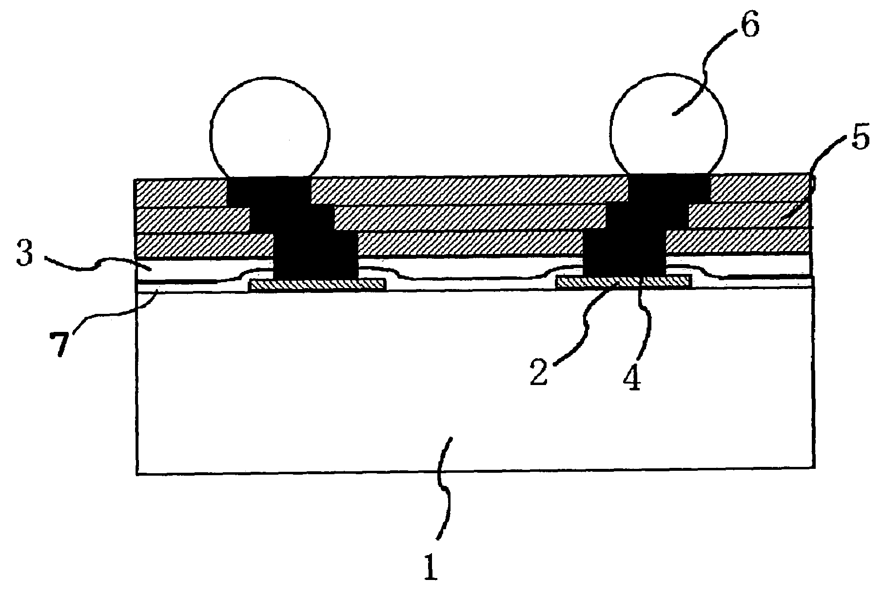
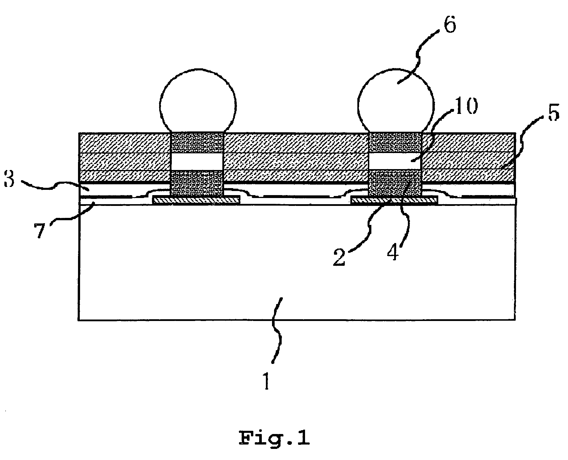
[0019]FIG. 1 is a cross-sectional view showing a semiconductor device according to a first embodiment of the present invention.

[0020]Electrode pads 2 are provided on an element-side surface of a semiconductor chip 1 on which an integrated circuit including semiconductor elements is formed. Then electrode pads 2 are electrically connected to the integrated circuit. A protective dielectric layer 3 and a coating layer 7 are formed around the electrode pads 2 such that apertures are formed in the protective dielectric layer 3 and the coating layer 7 so as to match the respective electrode pads 2. A post 4 as a connecting conductor is formed on each of the electrode pads 2 and includes a plurality of layers formed of same or different material, and at least one of the layers is formed as a stress-absorbing layer having lower hardness than other layer.

[0021]A stress-absorbing layer 10 is provided at the middle of the post 4. For example, a metal layer having a low Young's modulus, such as...

second embodiment

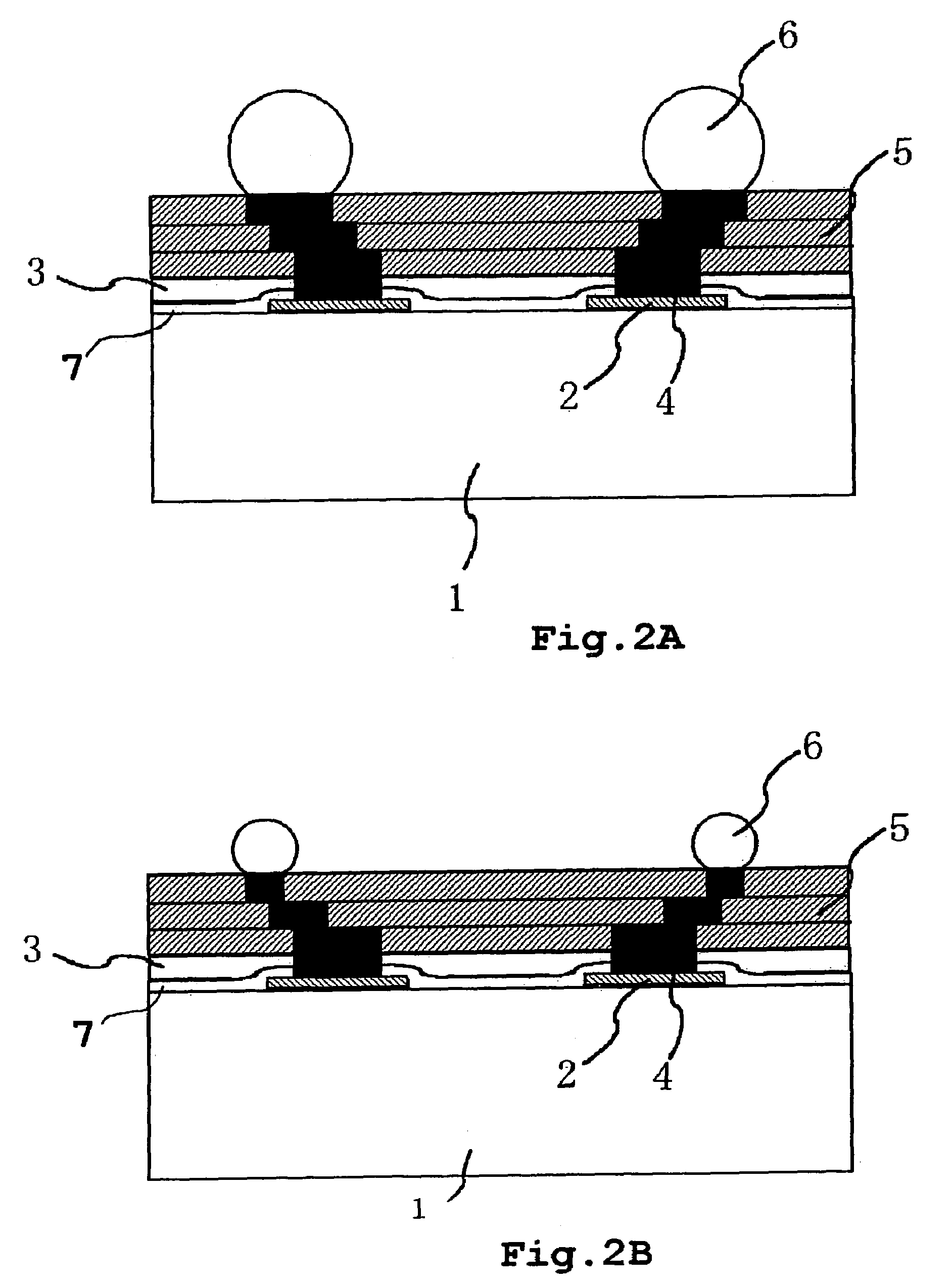
[0026]FIGS. 2A and 2B are cross-sectional views showing a semiconductor device according to a second embodiment of the present invention.

[0027]The electrode pads 2 are provided on the element-side surface of the semiconductor chip 1 on which an integrated circuit including semiconductor elements is formed. Then electrode pads 2 are electrically connected to the integrated circuit. The protective dielectric layer 3 and the coating layer 7 are formed around the electrode pads 2 such that apertures are formed in the protective dielectric layer 3 and the coating layer 7 so as to match the respective electrode pads 2.

[0028]A post 4 as a connecting conductor is formed on each of the electrode pads 2. The sealing resin 5 is formed around respective layer of the posts 4 so as to cover the posts 4.

[0029]More specifically, each of the posts 4 is divided into three layers, and the thus-divided layers are stacked in a staggered manner, to thereby alleviate the stress imposed on the posts 4. As ...


PUM


Abstract

There is described an improved semiconductor device of chip-scale package (CSP) comprising posts provided on respective electrode pads of a semiconductor chip, and solder balls which are provided on the respective posts as external terminals after the semiconductor chip has been encapsulated with resin while the posts are held in a projecting manner. The semiconductor device prevents occurrence of cracks, which would otherwise be caused by stress which is induced by a difference in coefficient of linear expansion between the semiconductor chip and the sealing resin and is imposed on the posts. In order to alleviate the stress imposed on the posts, a stress-absorbing layer formed from a metal layer having a low Young's modulus, such as gold (Au) or palladium (Pd), is interposed in the middle of each of the posts.

Description

BACKGROUND OF THE INVENTION[0001]1. Field of the Invention[0002]In association with miniaturization of and a reduction in the profile of an electronic component using an LSI, demand has recently arisen for miniaturizing an LSI package. A chip-scale package (CSP), which is identical in size with a semiconductor chip, has been developed.[0003]2. Background Art[0004]CSPs are classified into two types; that is, a CSP comprising a semiconductor chip electrically and mechanically connected to a printed board and a film carrier, with solder balls (bumps) being provided on the printed board and the film carrier as external terminals; and a CSP having neither a printed board nor a film carrier and comprising posts provided on respective electrode pads of a semiconductor chip, with solder balls being provided on the respective posts as external terminals after the semiconductor chip has been encapsulated with resin while the posts are held in a projecting manner.[0005]FIG. 3 is a cross-sectio...

Claims


Application Information

Patent Timeline
IPC IPC(8): H01L23/48H01L23/52H01L29/40H01L23/12H01L21/60H01L23/31H01L23/485
CPCH01L23/3114H01L24/10H01L24/13H01L23/3192H01L2924/01033H01L2224/13099H01L2924/01004H01L2924/01046H01L2924/01078H01L2924/01079H01L2924/14H01L2924/15174H01L2924/014H01L2924/00013H01L2924/01005H01L2924/00014H01L2924/00H01L2224/13H01L2224/05022H01L2224/05026H01L2224/0508H01L2224/05568H01L2224/05023H01L2224/05001H01L2224/05548H01L2224/056H01L24/05H01L2224/02125H01L2224/02379H01L2224/05144H01L2224/05164
Inventor WAKAMIYA, KEIICHIROYAMADA, SATOSHI
Owner RENESAS ELECTRONICS CORP
Why Eureka
Try Eureka