

IC layout physical verification method
a physical verification and layout technology, applied in the field of physical verification of layouts, can solve the problems of difficult to extract the geometric parameters of drawn inductor, and the designer finds it difficult to check the proper connectivity between multiple layers
- Summary
- Abstract
- Description
- Claims
- Application Information
AI Technical Summary
Problems solved by technology
Method used
Image

Examples
Embodiment Construction
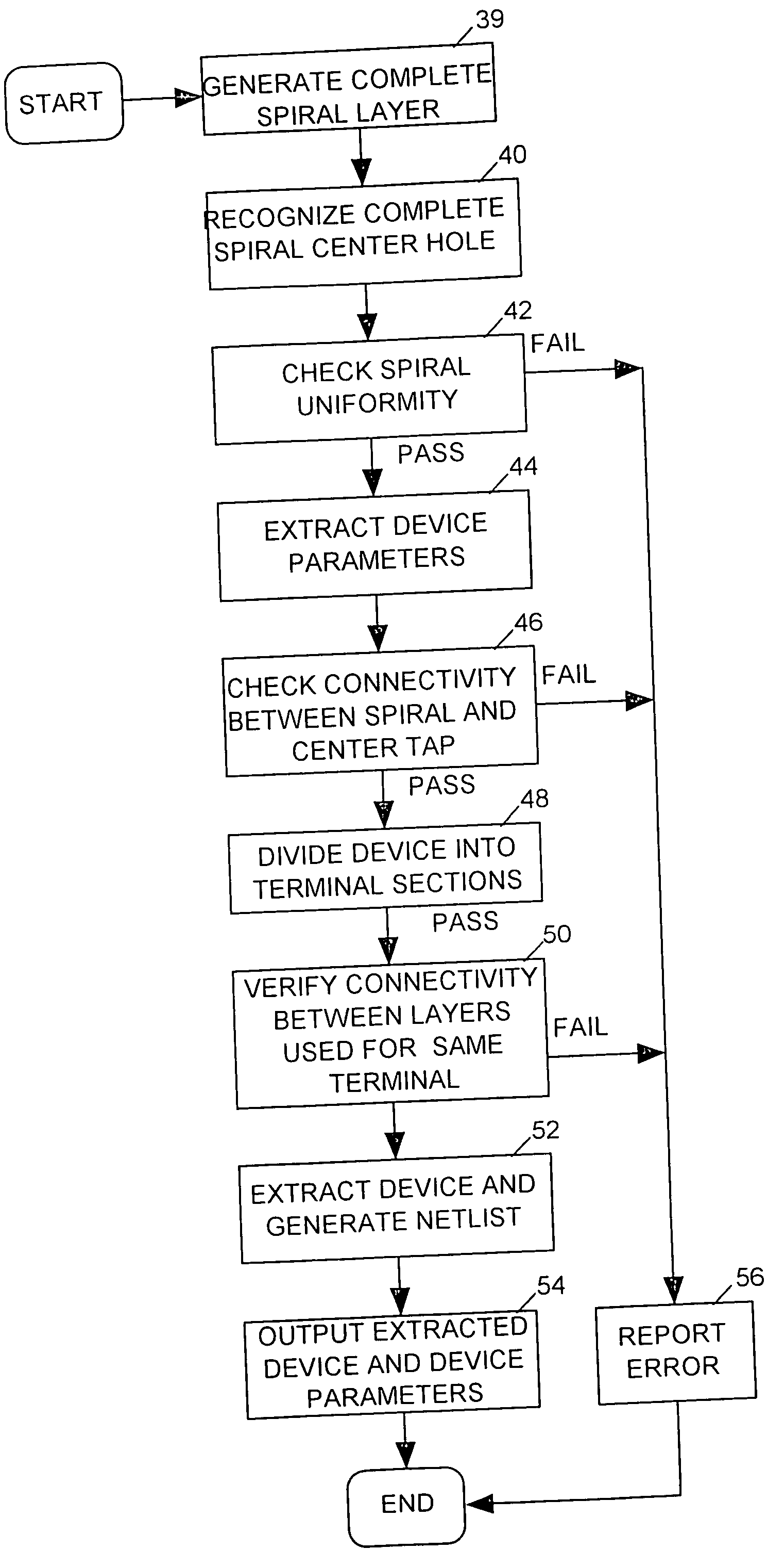
[0026] The present invention relates to a method for use by a “layout vs. schematic” (LVS) physical verification tool for identifying on-chip drawn inductors, for detecting connectivity and uniformity violations in the drawn inductors, and for measuring parameters that influence their inductance. The invention is suitably in the form of software stored on computer-readable media read and executed by a conventional computer acting as an LVS physical verification tool. Suitable computer-readable media for storing the software include, but are not limited to, compact disks, floppy disks, hard disks, and random access or read only memory. While the specification describes at least one exemplary embodiment of the invention considered a best mode of practicing the invention, those of skill in the art will appreciate that the invention need not be limited to the particular example(s) described below or to the manner in which they operate.
[0027] An integrated circuit (IC) designer may init...
PUM
 Abstract
Description
Claims
Application Information