Bonding structure and method for bonding members

Inactive Publication Date: 2005-10-20
SEIKO EPSON CORP
View PDF14 Cites 16 Cited by
  • Summary
  • Abstract
  • Description
  • Claims
  • Application Information

AI Technical Summary

Benefits of technology

[0056] The pressurization simultaneous with the heating can

Problems solved by technology

The method by allowing the fine conductive crystal grains to grow, however, cannot be applied to general bonding of members (for example, the bonding of semiconductor devices and substrates) in view of structure and strength.
T

Method used


Image

  • Bonding structure and method for bonding members
  • Bonding structure and method for bonding members
  • Bonding structure and method for bonding members

Examples


first embodiment

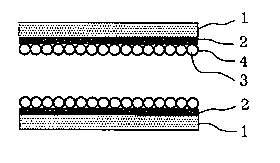
[0060]FIGS. 1A to 1D are schematic longitudinal sectional views showing the bonding steps of a method for bonding members according to a first embodiment of the present invention. Two members are bonded in FIGS. 1A to 1D, though this method may also be applied to the bonding of three or more members, for example the bonding of semiconductor devices to a substrate.

[0061] Referring to FIG. 1A, a receiving layer 2 is formed on each of two members 1. Examples of the material for the members 1 include metals, glass, synthetic resins, and semiconductors; substantially any solid may be used for the members 1 in the bonding structure and method of this embodiment. The members 1, which are flat in FIGS. 1A to 1D, may have a different shape. In addition, the two members 1 may be made of different materials, and may have, for example, wiring disposed thereon.

[0062] Typical examples of the material for the receiving layer 2 include polyamic acids, acrylic resin, alumina hydrate, calcium carbo...

second embodiment

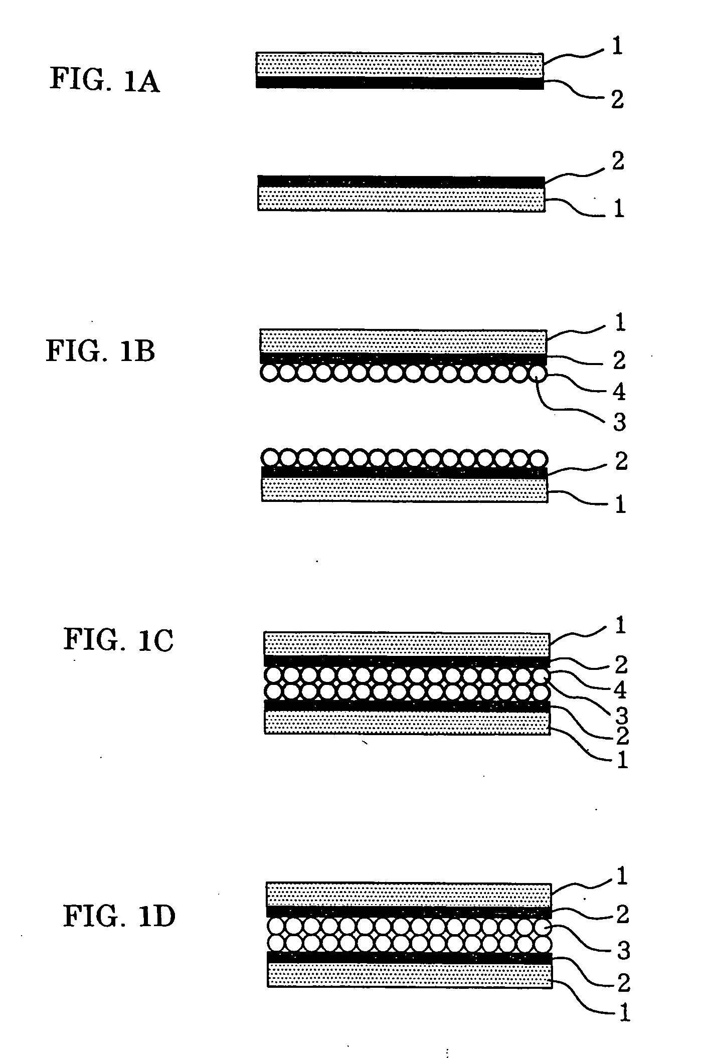
[0075]FIGS. 2A and 2B are schematic longitudinal sectional views showing the bonding steps of a method for bonding members according to a second embodiment of the present invention. In the second embodiment, a receiving structure 5 for holding the nanoparticles 3 is formed on the members 1 instead of the receiving layer 2 in the first embodiment. In the second embodiment, the bonding steps in FIGS. 1A and 1B in the first embodiment are replaced by those in FIGS. 2A and 2B, and the subsequent bonding steps are the same as those in FIGS. 1C and 1D. The other features of the second embodiment are the same as those of the first embodiment. In the following description, the same parts as in the first embodiment are indicated by the same reference numerals.

[0076] Referring to FIG. 2A, the receiving structure 5 is formed on each of the two members 1. Examples of the material for the members 1 include metals, glass, synthetic resins, and semiconductors; substantially any solid may be used ...

third embodiment

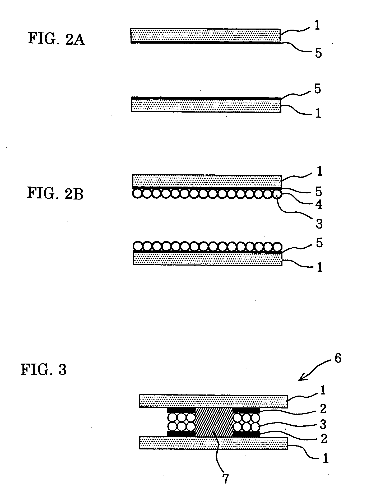
[0081]FIG. 3 shows an example of a product having a bonding structure according to a third embodiment of the present invention. Referring to FIG. 3, a liquid crystal panel 6 includes the members 1 bonded by the bonding method according to the first embodiment. As in FIG. 3, for example, the bonding structures according to the first and second embodiments of the present invention may be applied to a sealing structure for sealing a liquid crystal 7 in the liquid crystal panel 6.


PUM

PropertyMeasurementUnit
Structureaaaaaaaaaa

Abstract

A bonding structure includes members; nanoparticles bonding the members; and a receiving layer disposed on at least one of the members, holding the nanoparticles. Another bonding structure includes members; nanoparticles bonding the members; and a receiving structure formed on a surface of at least one of the members, holding the nanoparticles.

Description

BACKGROUND OF THE INVENTION [0001] 1. Field of the Invention [0002] The present invention relates to bonding structures and methods for bonding members and, particularly, to a bonding structure and method for bonding members with nanoparticles. [0003] 2. Description of the Related Art [0004] In a known microelectromechanical system (MEMS) according to, for example, PCT Japanese Translation Patent Publication No. 2003-519378 (see FIG. 1 of this publication), a first layer and a second layer are electrically connected by allowing fine conductive crystal grains to grow between these layers. [0005] According to another known bonding structure and method, members are bonded with nanoparticles disposed therebetween. [0006] The method by allowing the fine conductive crystal grains to grow, however, cannot be applied to general bonding of members (for example, the bonding of semiconductor devices and substrates) in view of structure and strength. [0007] This bonding structure and method usi...

Claims


Application Information

Patent Timeline
IPC IPC(8): B22F1/00B23K35/22B22F1/02B23K35/30B32B3/06B32B15/04B81C3/00C03C27/10H01L21/52H01L21/58H01L21/60H01L23/373
CPCB81C3/001H01L23/373H01L2224/743H01L24/31H01L24/81H01L24/83H01L2224/8121H01L2224/81815H01L2224/83193H01L2224/83801H01L2924/01002H01L2924/01005H01L2924/01012H01L2924/01013H01L2924/0102H01L2924/01029H01L2924/01033H01L2924/01047H01L2924/01056H01L2924/01078H01L2924/01079H01L24/29H01L2924/01006H01L24/743H01L2924/00D21D5/28B01F2035/3513B01F35/00
Inventor HASHIMOTO, NOBUAKI
Owner SEIKO EPSON CORP
Why Eureka
Try Eureka