LED array having array-based LED detectors

an array-based led detector and led array technology, which is applied in the direction of instruments, material analysis, electroluminescent light sources, etc., can solve the problems of sensor inability to determine the improper radiant output of the led array, the array may be operating improperly with respect to either/both the application parameters or/and the array's specifications, and the sensor cannot make adjustments except, so as to achieve no reduction or loss of total radiant flux

Active Publication Date: 2005-10-20
SILICON VALLEY BANK
View PDF99 Cites 85 Cited by
  • Summary
  • Abstract
  • Description
  • Claims
  • Application Information

AI Technical Summary

Benefits of technology

[0024] Utilizing detector diodes in the array to measure optical power and temperature has several advantages. One advantage is that the duty cycle and variance in the radiant intensity of the emitting array is substantially unaffected. Furthermore, since only a few diodes in the array are chosen for power monitoring there is virtually no reduction or loss of total radiant flux. Power monitoring and temperature sensing can be accomplished by providing the appropriate electronic circuitry to variably bias the proper diodes with additional circuitry to monitor the photocurrent. Therefore, using some of the diodes as photodetectors and temperature sensors provides a very efficient means of power monitoring and temperature sensing. In addition, locating detector diodes within the array provides an ideal location for monitoring power and temperature.

Problems solved by technology

An array may be operating improperly with respect to either / both the application's parameters or / and the array's specifications.
Accordingly, the sensors cannot determine where the LED array's radiant output may be improper and, as such, cannot make adjustments except across the entire array.
As well, by seeking to minimize or prevent detection of light energy reflected from the work piece or from external sources, control based on such light energy is precluded.
The respective sensor cannot determine where the LED array's radiant output may be improper across the implicated dimension and, as such, cannot make adjustments except across the entire set of LEDs associated with that fiber.
With photo detectors positioned in association with the output window, disadvantages include those set out above respecting other embodiments using light guide(s) to collect detected output radiation.
Such space generally is not desirable (i.e., typically, it is desirable to employ densely-packed LED arrays, wherein space between rows and columns of LEDs typically is insufficient to accept interposition of a semiconductor device, such as conventionally-sized sensor or detector).
The detecting group of LEDs cannot determine where the LED array's radiant output may be improper across any one or more rows of the emitting group and, as such, cannot make adjustments except for the entire group of emitting LEDs.
In addition, because of the potential for relatively substantial reduction of radiant output, it is generally not desirable to use any entire row in the LED array solely to detect, let alone using half of all rows of the LED array for detection.

Method used


Image

  • LED array having array-based LED detectors
  • LED array having array-based LED detectors
  • LED array having array-based LED detectors

Examples


Embodiment Construction

[0034] Representative embodiments of the present invention are shown in FIGS. 1-7 wherein similar features share common reference numerals.

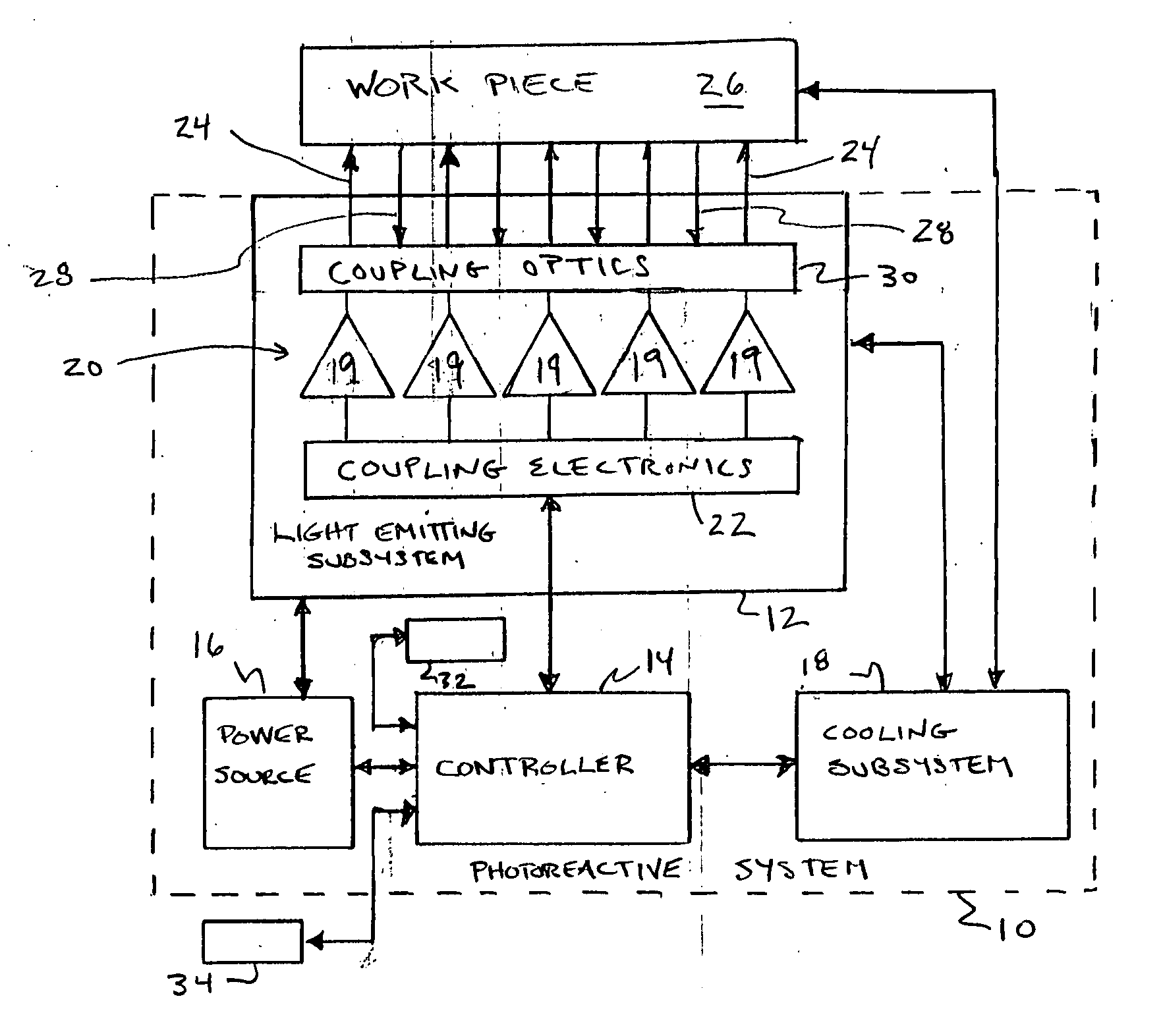
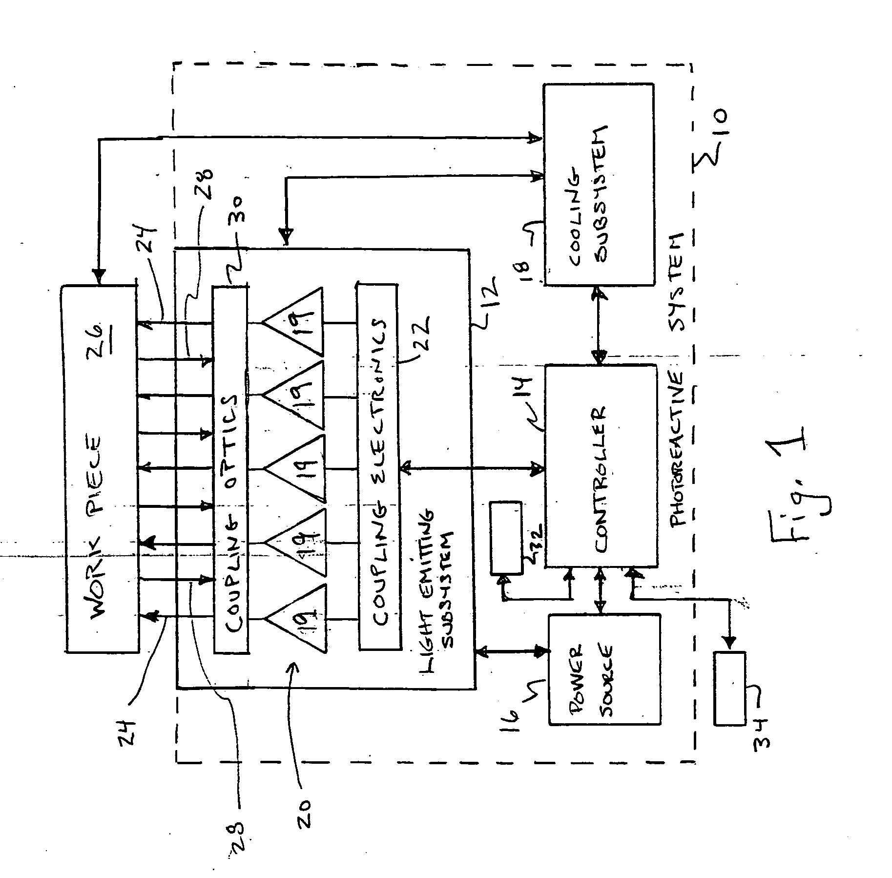
[0035]FIG. 1 is a block diagram of a photoreactive system 10 in accordance with the invention. In this example embodiment, the photoreactive system 10 comprises a light emitting subsystem 12, a controller 14, a power source 16 and a cooling subsystem 18.

[0036] The light emitting subsystem 12 preferably comprises a plurality of semiconductor devices 19. Selected of the plurality of semiconductor devices 19 are implemented to provide radiant output 24. The radiant output 24 is directed to a work piece 26. Returned radiation 28 may be directed back to the light emitting system 12 from the work piece 26 (e.g., via reflection of the radiant output 24).

[0037] The radiant output 24 preferably is directed to the work piece 26 via coupling optics 30. The coupling optics 30, if used, may be variously implemented. As an example, the coupling optics may i...


PUM


Abstract

The present invention provides an optical system having an array of light emitting semiconductor devices to performing an operation that have multiple characteristics associated with performing the operation. The array includes at least one detector located within the array to selectively monitor multiple characteristics of the light emitting semiconductor devices and is configured to generate a signal corresponding to the selected characteristic. A controller is configured to control the light emitting semiconductor devices in response to the signal from the at least one detector. At least one of the multiple characteristics may be concentrated at an area of the array and the at least one detector may be located within the array at the area of the array to selectively monitor characteristic that is concentrated at the area of the array.

Description

[0001] This invention claims the benefit of co-pending U.S. Provisional Application No. 60 / 558,205, entitled LED Array With Dual-Use LEDs For Both Illumination And Optical Detection, filed on Mar. 30, 2004, the entire disclosure of which is hereby incorporated by reference and set forth in its entirety for all purposes.BACKGROUND OF THE INVENTION [0002] Light-emitting semiconductor devices may be arranged in various configurations, such as arrays, for lighting applications. These applications generally have associated parameters (e.g., a photoreaction may entail provision of one or more levels of radiant power, at one or more wavelengths, applied over one or more periods of time). In these applications, the light emitting semiconductor devices generally are employed to provide radiant output and otherwise operate in accordance with various, desired characteristics, e.g., temperature, spectral distribution and radiant power. At the same time, the light emitting semiconductor devices ...

Claims


Application Information

Patent Timeline
Patent Type & Authority Applications(United States)
IPC IPC(8): H01L27/00
CPCH05B33/0851H05B33/0827H05B45/18H05B45/12H05B45/46
Inventor OLSON, STEVEN J.ANDERSON, DUWAYNE R.CULTER, ROBERT G.OWEN, MARK D.
Owner SILICON VALLEY BANK
Why Eureka
Try Eureka