Piezoelectric actuator, inkjet head and fabrication methods thereof

Inactive Publication Date: 2005-10-20
NAT INST OF ADVANCED IND SCI & TECH
View PDF9 Cites 24 Cited by
  • Summary
  • Abstract
  • Description
  • Claims
  • Application Information

AI Technical Summary

Benefits of technology

[0047] In the 14th or 22nd mode of the present invention, the substrate is formed by means of a conductive material and, by using the same as one electrode for applying an electric field to the piezoelectric material layers, it is not necessary to especially provide one electrode, which is advantageous from a fabrication cost standpoint.
[0048] In the 24th mode of the present invention, the value of the ratio between the Vickers hardness Hv (b) of the film-deposition permitting region and the compressive breaking strength Gv (p) of the particles in unit of GPa is in the range 0.10≦Gv (p)/Hv (b)×100≦3.08 and the ratio between the Vickers hardness Hv (b) of the film-deposition inhibiting region and the compressive breaking strength Gv (p) of the particles in unit of GPa is a value less than 0.10 or exceeding 3.08, and, hence, the deposition of the piezoelectric material layer on the film-deposition inhibiting region can be reliably inhibited and the adhesion (film deposition properties) of the piezoelectric material layer to the film-deposition permitting region can be ensured.
[0049] In the 25th mode of the present invention, the value of the ratio between the Vickers hardness Hv (b) of the film-deposition permitting region

Problems solved by technology

However, in this case, vibrations are transmitted to the periphery of the bent part of the piezoelectric material layer and, as a result, there is a variation in the ejection speed and volume, and so forth when the ink is ejected from an adjacent pressure cha

Method used


Image

  • Piezoelectric actuator, inkjet head and fabrication methods thereof
  • Piezoelectric actuator, inkjet head and fabrication methods thereof
  • Piezoelectric actuator, inkjet head and fabrication methods thereof

Examples


first embodiment

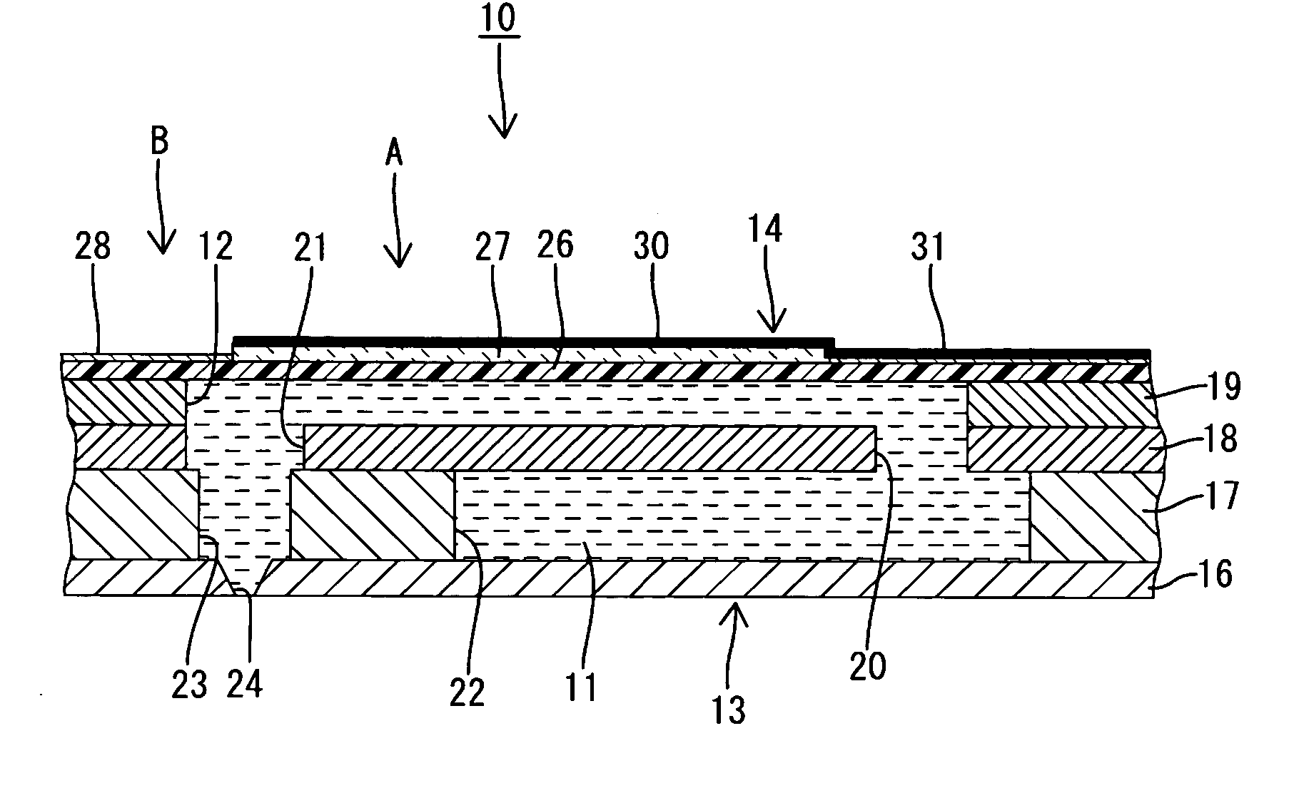
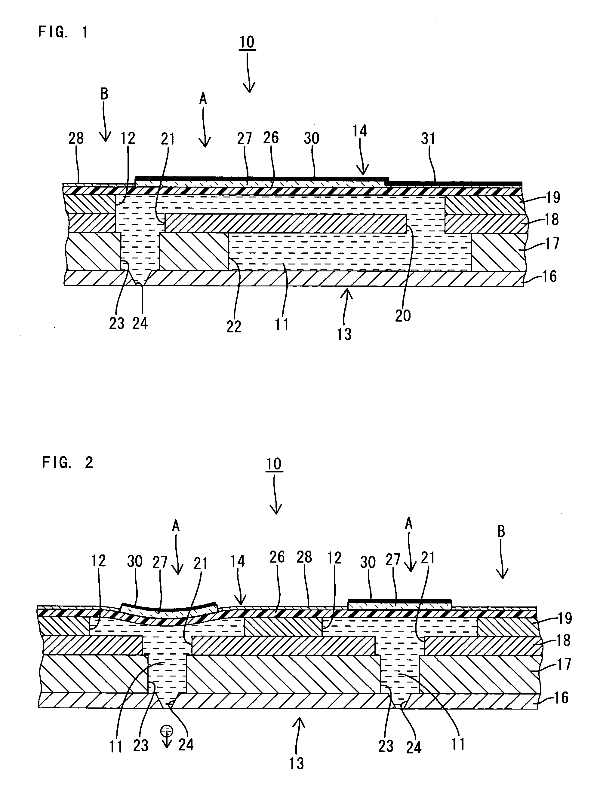
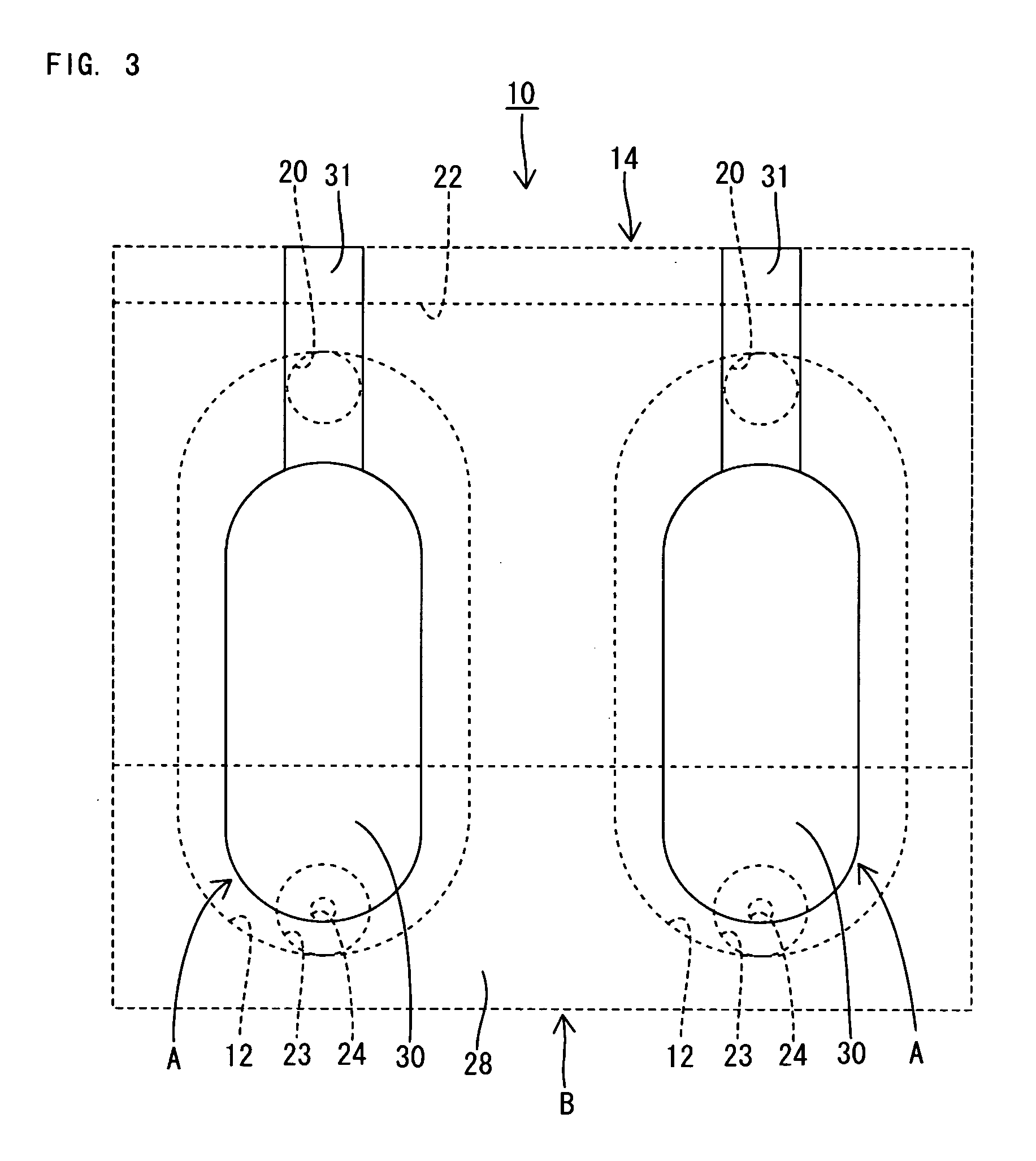
[0069] The first embodiment of the present invention will be described with reference to FIGS. 1 to 4, 5A, 5B and 5C. FIG. 1 is a cross-sectional view in which an inkjet head 10 of this embodiment (corresponds to the ‘inkjet head’ of the present invention) is sectioned in the length direction of a pressure chamber 12. FIG. 2 is a cross-sectional view in which the inkjet head 10 is sectioned in the breadth direction of the pressure chamber 12. FIG. 3 is a planar view of the inkjet head 10 that shows a part of the inkjet head 10 together with each of the drawings.

[0070] The inkjet head 10 comprises an ink flow path formation member 13 that comprises a plurality of pressure chambers 12 with a form in which ink 11 is accommodated and an upper face is open, and an actuator unit 14 that is secured to the upper surface of the ink flow path formation member 13.

[0071] The ink flow path formation member 13 has a planar shape overall and is constituted such that a nozzle plate 16, manifold p...

second embodiment

[0162] The second embodiment of the present invention will be described below with reference to FIGS. 7 and 8. Further, in the following description, the same reference numerals have been assigned to the constituent parts that are the same as those of the first embodiment and a description thereof is omitted here.

[0163] In the inkjet head 50 of the present embodiment, a different hardness material layer 52, constituting the film-deposition inhibiting region B on the substrate 26 of the actuator unit 51, is conductive. As a result, one ends of conductive paths 54 of a flat cable 53, which is connected to the driver circuit (not shown), is connected to individual electrodes 30, which are formed on the upper surface of each piezoelectric material layers 27 instead of being connected to the lead portions 31 of the first embodiment. The remaining structure is substantially similar to that of the first embodiment.

[0164] The substrate 26 is formed from a material that is the same as that...

third embodiment

[0168] The third embodiment of the present invention will be described below with reference to FIGS. 9 and 10A, 10B, 10C and 10D. Further, in the following description, the same reference numerals have been assigned to the constituent parts that are the same as those of the first embodiment and a description thereof is omitted here.

[0169] In the case of the inkjet head 60 of this embodiment, the roughness of the surface of the film-deposition inhibiting region B where the piezoelectric material layer 27 is not formed on the surface of a substrate 62 of an actuator unit 61 is made larger than the surface roughness of the film-deposition permitting regions A where the piezoelectric material layers 27 are formed. That is, in this embodiment, the film-deposition permitting regions A and the film-deposition inhibiting region B are made different by changing the mutual surface roughness. The film-deposition permitting regions A are afforded such a surface roughness that, in the piezoelec...


PUM

PropertyMeasurementUnit
Speedaaaaaaaaaa
Speedaaaaaaaaaa
Speedaaaaaaaaaa

Abstract

A piezoelectric material layer is easily formed on a partial region of the substrate surface. By forming a different hardness material layer that has a different hardness from that of the substrate in the form of a pattern on the surface of the substrate, a film-deposition permitting region A to which particles of a piezoelectric material in a carrier gas adhere in a form of a film and a film-deposition inhibiting region B which inhibits the formation of a film are provided. Further, when a carrier gas containing particles of a piezoelectric material are ejected onto the surface of the substrate by means of AD, a film-like piezoelectric material layer is formed as a result of the adhesion of the particles in the film-deposition permitting region A. As a result, the piezoelectric material layer can be formed easily in a partial region of the surface of the substrate.

Description

BACKGROUND OF THE INVENTION [0001] 1. Field of the Invention [0002] The present invention relates to a piezoelectric actuator that is fabricated by using so-called aerosol deposition (AD) that performs film deposition by mixing a raw material with a gas and ejecting the mixture from a nozzle so that the same collides with a substrate, and to an inkjet head and fabrication methods thereof. [0003] 2. Description of the Related Art [0004] As an example of a piezoelectric actuator that is used in an inkjet head or the like, there is a piezoelectric actuator that comprises an ink flow path formation member in which a plurality of pressure chambers is formed, wherein a substrate that constitutes a portion of the wall surface of each of the pressure chambers is bent by means of a piezoelectric material layer that is provided on the substrate so that ink in the pressure chambers is ejected out from a nozzle that communicates with the pressure chamber (See Japanese Patent Application Laid Op...

Claims


Application Information

Patent Timeline
IPC IPC(8): B41J2/14B41J2/16H01L41/08H01L41/22
CPCB41J2/14233Y10T29/49128B41J2/1623B41J2/1626B41J2/1631B41J2/1642B41J2/1643B41J2/1645B41J2/1646H01L41/0805H01L41/314H01L41/319Y10T29/4913Y10T29/49401Y10T29/42Y10T29/49005Y10T29/49007B41J2/161H10N30/1051H10N30/074H10N30/079
Inventor SUGAHARA, HIROTOKOBAYASHI, KAZUOYASUI, MOTOHIROAKEDO, JUNBABA, SOU
Owner NAT INST OF ADVANCED IND SCI & TECH
Why Eureka
Try Eureka