
Drive circuit with offset compensation capability, and liquid crystal display using the same

a technology of offset compensation and liquid crystal display, which is applied in the direction of instruments, static indicating devices, transportation and packaging, etc., can solve the problems of affecting the accuracy of offset compensation circuit cancellation, affecting the voltage of capacitors, and increasing the area occupied by offset compensation circuits, so as to achieve accurate cancellation of offset voltage and small area

Inactive Publication Date: 2005-10-20
MITSUBISHI ELECTRIC CORP
View PDF2 Cites 8 Cited by
  • Summary
  • Abstract
  • Description
  • Claims
  • Application Information

AI Technical Summary

Benefits of technology

[0007] In view of the foregoing, a major object of the present invention is to provide a drive circuit having offset compensation capability that occupies a small area and can accurately cancel an offset voltage, and a liquid crystal display using the same.
[0009] As such, the gate electrode of the input transistor of the drive circuit is used as one electrode of an offset-compensating capacitor. Accordingly, the parasitic capacitance of the gate of the input transistor can be made small, and the offset voltage can be compensated accurately, without increasing the area occupied.
[0011] As such, one electrode of the offset-compensating capacitor, connected to the gate electrode of the input transistor of the drive circuit, is provided between two other electrodes. Accordingly, the parasitic capacitance of the gate of the input transistor can be made small, and the offset voltage can be compensated accurately, without increasing the area occupied.

Problems solved by technology

In the conventional offset compensation circuit, however, there occurs a loss of the voltage of the capacitor due to an influence of parasitic capacitance of the input node of the drive circuit, hindering accurate cancellation of the offset voltage.
To do so, however, the area of the capacitor needs to be made large, which leads to an increase of the area occupied by the offset compensation circuit.
This poses a serious problem particularly when using the offset compensation circuit for a data line drive circuit of a liquid crystal display, since a great number of offset compensation circuits are necessary.

Method used


Image

  • Drive circuit with offset compensation capability, and liquid crystal display using the same
  • Drive circuit with offset compensation capability, and liquid crystal display using the same
  • Drive circuit with offset compensation capability, and liquid crystal display using the same

Examples


first embodiment

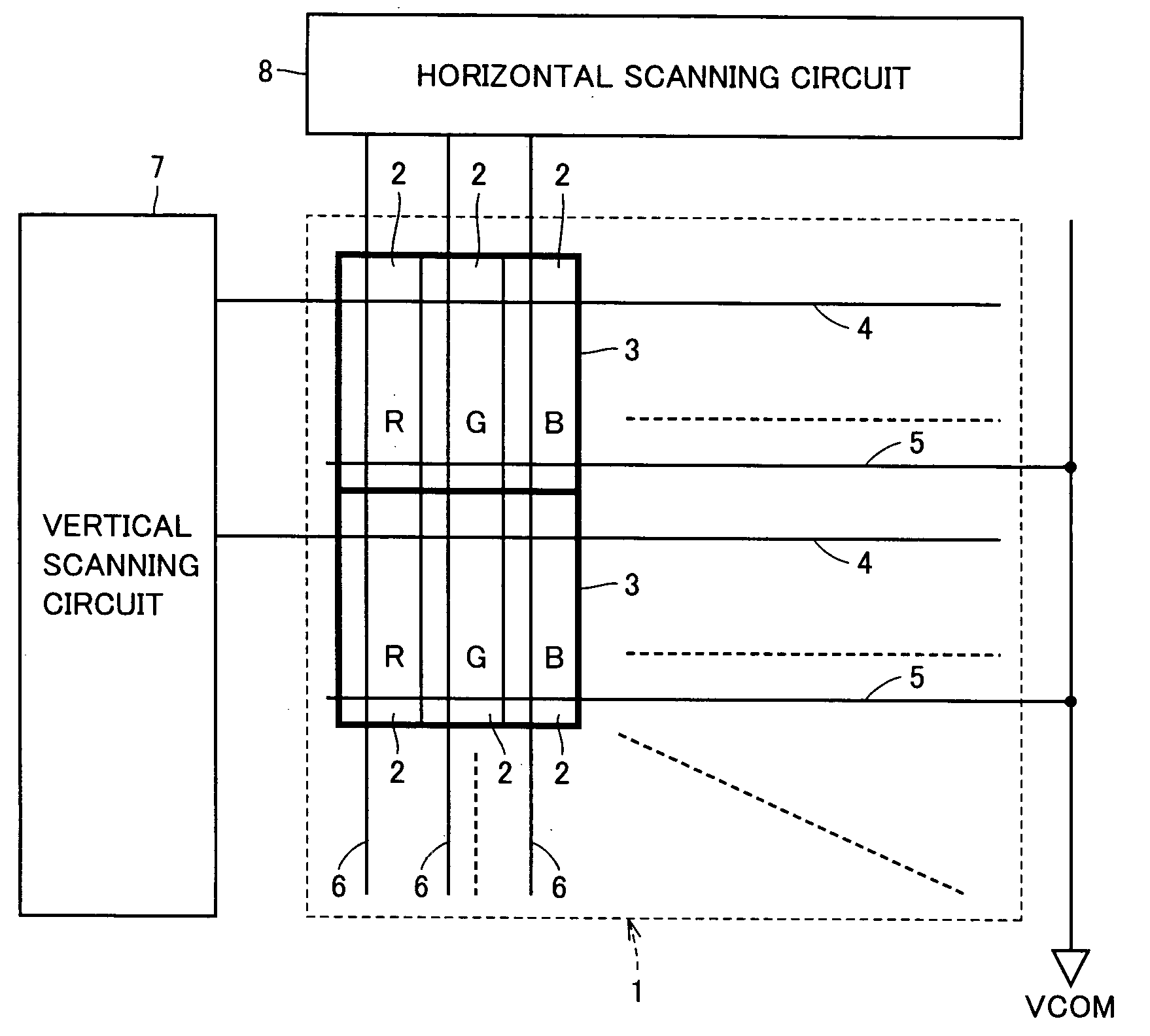
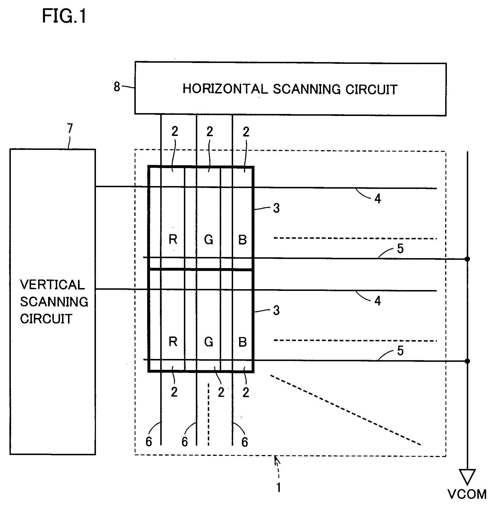
[0028]FIG. 1 shows a configuration of a color liquid crystal display according to the first embodiment of the present invention. Referring to FIG. 1, the color liquid crystal display includes a liquid crystal panel 1, a vertical scanning circuit 7 and a horizontal scanning circuit 8, and is provided to a mobile telephone, for example.

[0029] Liquid crystal panel 1 includes a plurality of liquid crystal cells 2 arranged in rows and columns, a gate line 4 and a common potential line 5 provided corresponding to each row, and a data line 6 provided corresponding to each column. In each row, liquid crystal cells 2 are grouped into three each in advance. Three liquid crystal cells 2 in each group are provided with color filters of R, G and B, respectively. Three liquid crystal cells 2 in each group constitute one pixel 3.

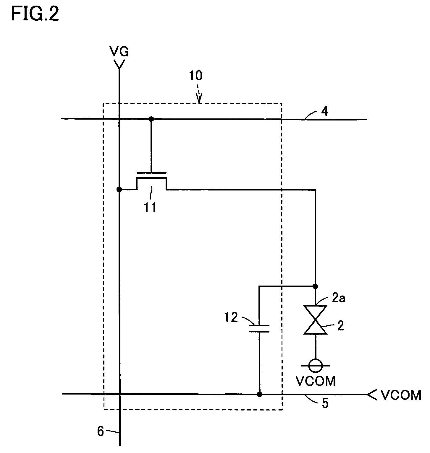
[0030] A liquid crystal drive circuit 10 is provided for each liquid crystal cell 2, as shown in FIG. 2. Liquid crystal drive circuit 10 includes an N type transistor 11...

second embodiment

[0054]FIG. 9 shows a main part of an analog amplifier unit circuit according to the second embodiment of the present invention. Referring to FIG. 9, the analog amplifier unit circuit of the present embodiment differs from the analog amplifier unit circuit shown in FIG. 4 in that drive circuit 25 is replaced with a drive circuit 40.

[0055] Drive circuit 40 includes a constant current circuit 41 and a P type transistor 42. Constant current circuit 41 is connected between a line of a high potential VH2 and node N22, and causes a current of a prescribed value to flow from the line of high potential VH2 to node N22. P type transistor 42 is connected between node N22 and a line of low potential VL2, and has its gate electrode connected to node N21.

[0056] The drive current of P type transistor 42 is set sufficiently greater than the current value of constant current circuit 41. Thus, P type transistor 42 carries out the source-follower operation, and potential V22 of node N22 becomes: V22...

third embodiment

[0072]FIG. 16 shows a configuration of an analog amplifier unit circuit 80 according to the third embodiment of the present invention. Referring to FIG. 16, in this analog amplifier unit circuit 80, one terminal of switch S1 of analog amplifier unit circuit 20 in FIG. 4 is connected to a node N80 of a reference potential VR, instead of input node N20. Reference potential VR may be provided directly from the outside of the liquid crystal display, or may be provided from a power supply circuit of low output impedance provided within the liquid crystal display. Input node N20 is connected to one terminal of switch S3. The way of controlling switches S1-S4 is as described in the first embodiment.

[0073] Effects of analog amplifier unit circuit 80 are now explained. Firstly, when switches S1 and S2 are turned on, input potential V21 of drive circuit 25 attains reference potential VR, and output potential V22 of drive circuit 25 becomes: V22=V21−VTN=VR−VTN. Capacitors 23, 24 are charged t...


PUM

PropertyMeasurementUnit
Electrical conductivityaaaaaaaaaa
Electric potential / voltageaaaaaaaaaa
Capacitanceaaaaaaaaaa

Abstract

In an analog amplifier unit circuit included in a color liquid crystal display, an aluminum interconnection is formed to cover a gate electrode of an input transistor of a drive circuit, and capacitance between the gate electrode and the aluminum interconnection is used as an offset-compensating capacitor. Thus, the parasitic capacitance of the gate electrode of the input transistor can be made small, and the offset voltage can be canceled accurately, without increasing the area occupied by a capacitor.

Description

BACKGROUND OF THE INVENTION [0001] 1. Field of the Invention [0002] The present invention relates to a drive circuit having offset compensation capability and a liquid crystal display using the same. More particularly, the present invention relates to a drive circuit having offset compensation capability that outputs a potential corresponding to an input potential, and a liquid crystal display using the same. [0003] 2. Description of the Background Art [0004] There has conventionally been proposed an offset compensation circuit that cancels an offset voltage of a drive circuit. In the offset compensation circuit, a capacitor is charged to the offset voltage, and the capacitor is connected to an input node of the drive circuit to compensate the offset voltage (see, e.g., Japanese Patent Laying-Open No. 2000-114889). [0005] In the conventional offset compensation circuit, however, there occurs a loss of the voltage of the capacitor due to an influence of parasitic capacitance of the i...

Claims


Application Information

Patent Timeline
IPC IPC(8): G02F1/133G02F1/1362G09G3/36H03F3/50
CPCG02F1/136213G09G2310/027G09G3/3688B65B11/025B65B41/12B65B61/10B65H35/06B65H81/00B65H2301/51532B65H2801/81
Inventor TOBITA, YOUICHI
Owner MITSUBISHI ELECTRIC CORP
Learn More