Optical inspection equipment for semiconductor wafers with precleaning

a technology of optical inspection equipment and semiconductor wafers, applied in the direction of optical radiation measurement, semiconductor/solid-state device testing/measurement, instruments, etc., can solve the problems of inability to achieve the desired effect, damage to the gate dielectric, and cleaning procedures which require contact with the wafer, etc., to achieve the effect of improving the repeatability of the resul

Inactive Publication Date: 2005-10-20
THERMA WAVE INC
View PDF18 Cites 7 Cited by
  • Summary
  • Abstract
  • Description
  • Claims
  • Application Information

AI Technical Summary

Benefits of technology

[0018] Once the wafer has been treated by the microwave radiation or radiant heating, it can be measured using a conventional optical metrology tool. As described above, one or more probe beams are caused to reflect off the sample and changes in the reflected probe beam or beams are monitored to derive information about the sample. It may be desirable to perform the measurement in a vacuum or inert gas environment. It may also be desirable to make the measurement in the same chamber where the wafer was exposed to the cleaning step to minimize any build up of the contamination layer while the wafer is being transferred. It would also be possible to measure the wafer at the same time it is being exposed to the microwave radiation or radiant heating.
[0020] If a radiant heat source is used, it should operate in the one to ten micron wavelength regime. It is believed that the cleaning effect achieved using a radiant heat source at this wavelength excites the vibrational bands in the water molecules helping to drive it into the vapor state thereby carrying off any associated hydrocarbon contamination.
[0021] In one embodiment of the invention, cleaning is achieved by combining the microwave radiation and the radiant heating. Using two cleaning sources permits the optimization of the parameters of both modalities to maximize cleaning while minimizing damage to the wafer or deposited thin films.
[0023] It may also be desirable to initially expose the wafer to a high humidity environment before cleaning the wafer with microwave energy. Such a high humidity environment would increase the amount of water molecules attached to the wafer. When the wafer is subsequently exposed to the microwave radiation, the vaporization of these added water molecules may actually enhance the removal of other contaminants thereby improving the cleaning action.

Problems solved by technology

As thin films and thin film stacks have become more numerous and complex, the industry has begun developing composite measurement tools that have multiple measurement modules within a single device.
There is a need to measure the thickness of these very thin layers with a precision and repeatability to better than 0.1 Å. While the Opti-Probe device is capable of making such measurements with the necessary precision, problems have arisen with respect to repeatability, especially with ultrathin films.
However, any cleaning procedures which requires contact with the wafer, such as cleaning solutions, would not be desirable at this stage of fabrication since it can damage or contaminate the gate dielectric or the wafer.
However, the temperature required to clean the wafer would be relatively high and this high temperature can damage the gate dielectric.

Method used


Image

  • Optical inspection equipment for semiconductor wafers with precleaning
  • Optical inspection equipment for semiconductor wafers with precleaning
  • Optical inspection equipment for semiconductor wafers with precleaning

Examples


Embodiment Construction

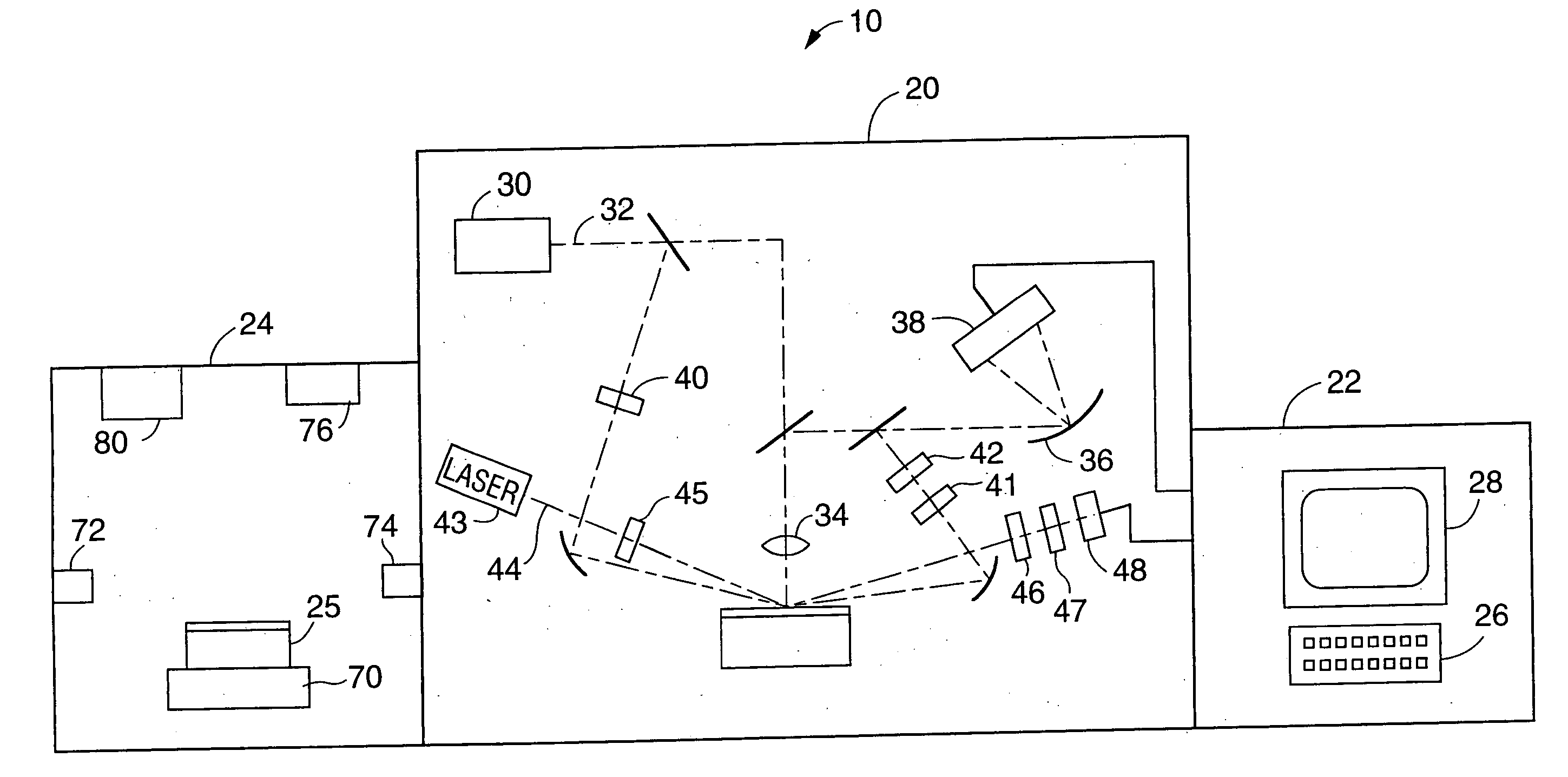
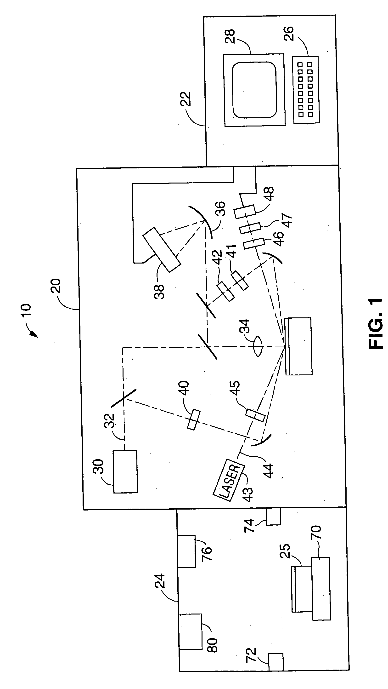
[0028]FIG. 1 is a simplified block diagram of a device 10 made in accordance with the subject invention. This device includes a measurement station 20 and a computer processor acting as a controller and computational module 22. In the preferred embodiment, the device also includes a microwave or radiant heating module 24 for holding a wafer 25. It should be noted that in the broadest sense, the method of the subject invention can be performed with separate cleaning and optical measurement devices. However, there are many reasons why the two tools should be combined in a single instrument. For example, automatic wafer transport can be provided between the cleaning module and the measurement module. Besides eliminating human handling, direct wafer transfer can reduce the time between cleaning and measurement thereby minimizing the regrowth of a contaminant layer prior to the measurement. In addition, a single tool has a smaller footprint and therefore takes up less space in the semico...


PUM

PropertyMeasurementUnit
wavelengthaaaaaaaaaa
thicknessaaaaaaaaaa
skin depthaaaaaaaaaa

Abstract

A method for improving the measurement of semiconductor wafers is disclosed. In the past, the repeatability of measurements was adversely affected due to the unpredictable growth of a layer of contamination over the intentionally deposited dielectric layers. Repeatability can be enhanced by removing this contamination layer prior to measurement. This contamination layer can be effectively removed in a non-destructive fashion by subjecting the wafer to a cleaning step. In one embodiment, the cleaning is performed by exposing the wafer to microwave radiation. Alternatively, the wafer can be cleaned with a radiant heat source. These two cleaning modalities can be used alone or in combination with each other or in combination with other cleaning modalities. The cleaning step may be carried out in air, an inert atmosphere or a vacuum. Once the cleaning has been performed, the wafer can be measured using any number of known optical measurement systems.

Description

PRIORITY [0001] This application is a continuation of U.S. patent application Ser. No. 10 / 717,316, filed Nov. 19, 2003, which is in turn a continuation of U.S. patent application Ser. No. 09 / 294,869, filed Apr. 20, 1999, now U.S. Pat. No. 6,714,300, which claimed the benefit of U.S. Provisional Application 60 / 102,167, filed Sep. 28, 1998, said application being incorporated herein by reference.TECHNICAL FIELD [0002] The subject invention relates to optical inspection equipment used to evaluate parameters of thin films on semiconductor wafers. The subject device includes a cleaning module for reducing contaminants on the surface of the wafer prior to measurement to improve the accuracy and repeatability of the optical measurements. In the preferred embodiments, the cleaning module includes either or both of a microwave radiation source and a radiant heating source. BACKGROUND OF THE INVENTION [0003] For many years, devices have existed for evaluating parameters of a semiconductor waf...

Claims


Application Information

Patent Timeline
Patent Type & Authority Applications(United States)
IPC IPC(8): G01J4/04G01N21/21G01N21/95H01L21/00H01L21/306H01L21/66
CPCG01N21/211G01N21/9501G01N2201/0227G01N2201/023H01L22/20H01L21/02054H01L21/67028H01L21/67115H01L21/02046
Inventor ROSENCWAIG, ALLANWEI, LANHUA
Owner THERMA WAVE INC
Why Eureka
Try Eureka