Alternating asymmetrical plasma generation in a process chamber

a plasma generation and process chamber technology, applied in the field of plasma processing systems, can solve the problems of increasing the ion density in places, affecting so as to improve the uniformity of the plasma process

Inactive Publication Date: 2005-11-03
APPLIED MATERIALS INC
View PDF29 Cites 123 Cited by
  • Summary
  • Abstract
  • Description
  • Claims
  • Application Information

AI Technical Summary

Benefits of technology

[0010] Embodiments of the invention provide an apparatus for plasma processing a substrate, wherein the apparatus includes first and second plasma controlling devices that are in communication with a processing region of a plasma chamber. The first plasma controlling device and second plasma controlling device are connected to a first RF power source and a second RF power source, respectively. A controller that is connected...

Problems solved by technology

This is undesirable for some processing sequences, because the plasma uniformity over the surface of the substrate generated in a particular processing chamber may be acceptable for one portion of a sequence, while causing substrate damage during another portion of the sequence.
However, varying the gas flow is also undesirabl...

Method used


Image

  • Alternating asymmetrical plasma generation in a process chamber
  • Alternating asymmetrical plasma generation in a process chamber
  • Alternating asymmetrical plasma generation in a process chamber

Examples


example 1

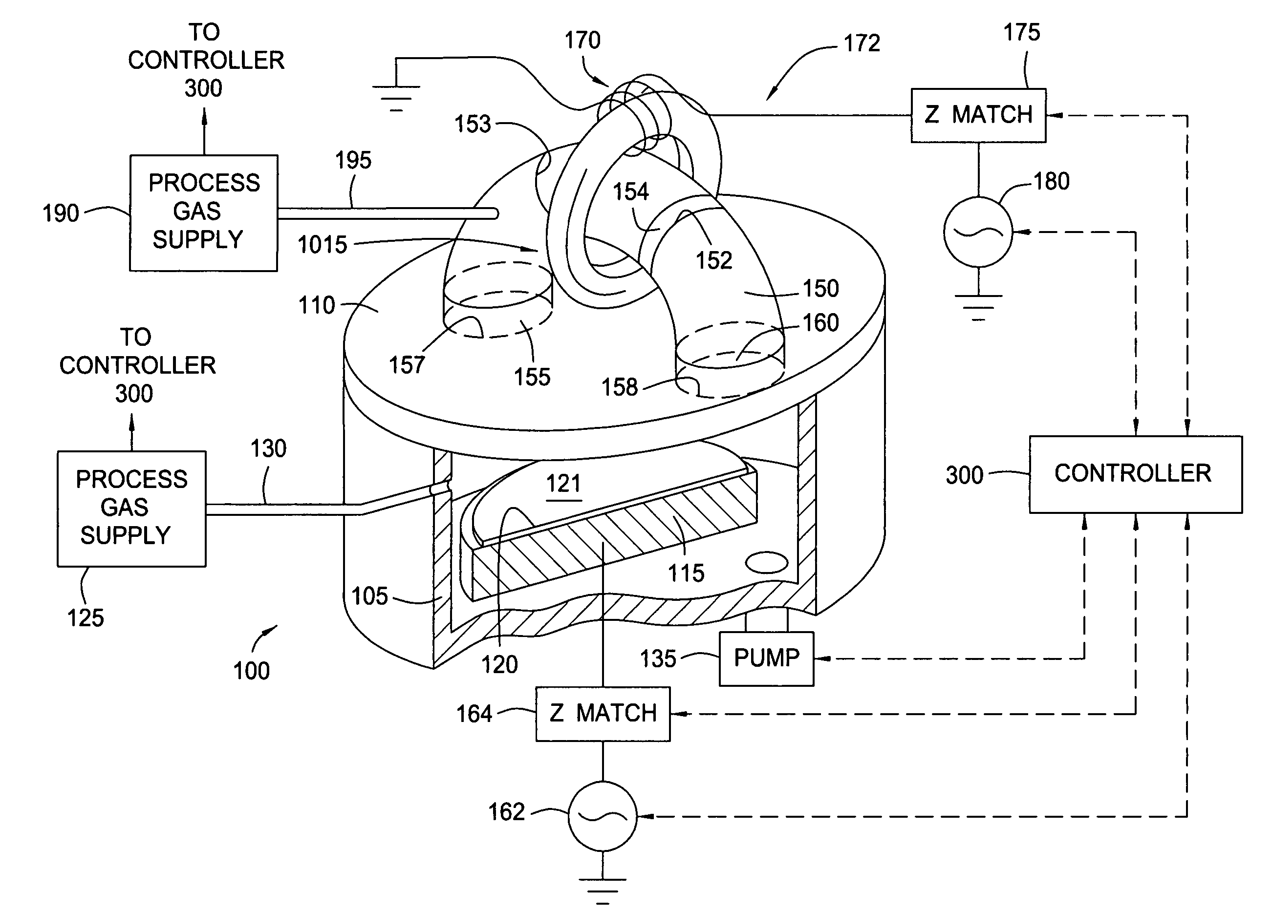
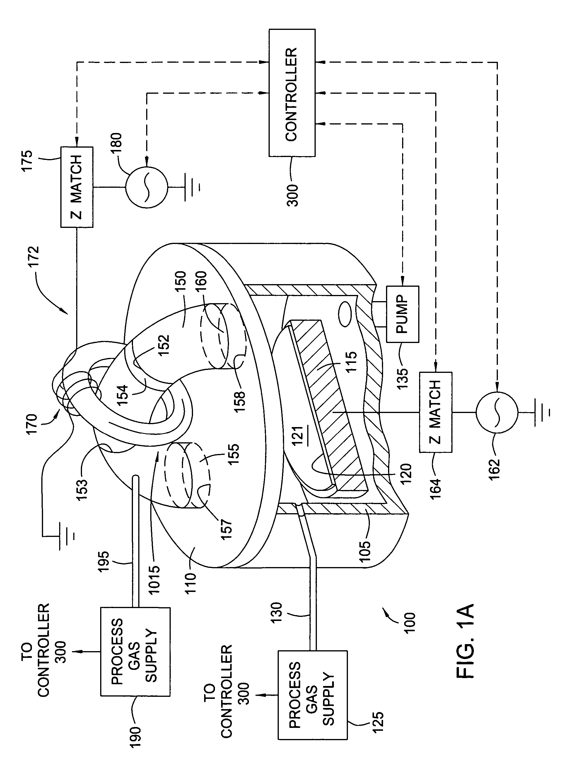
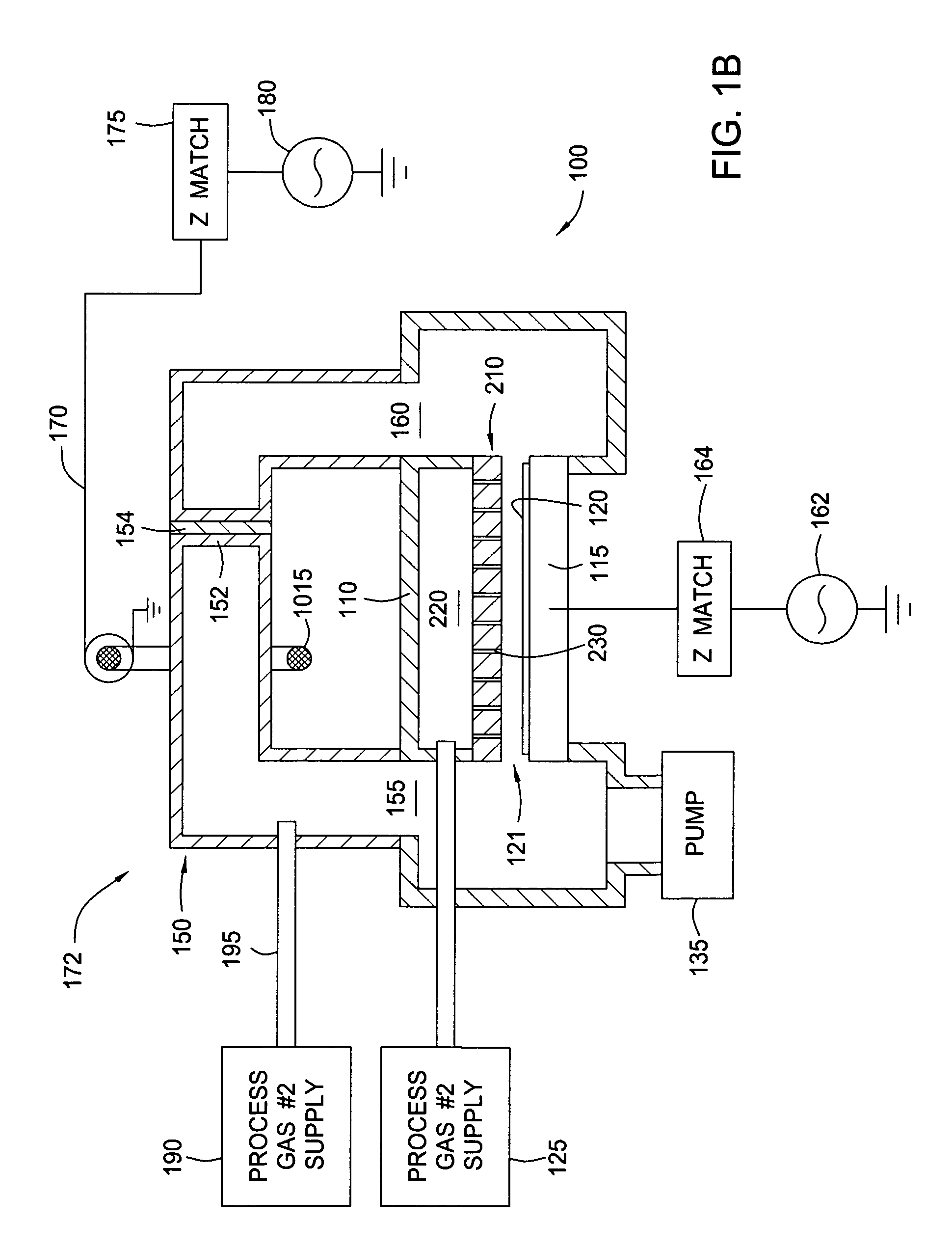
[0104] Examples of different plasma processing recipes utilizing an amplitude modulation of RF power delivered to an orthogonal two plasma controlling device torroidal source are described below for a silicon dioxide etching process. The general process parameters used to etch the surface of a substrate having a silicon dioxide thickness of 20,000 Angstroms are as follows: a chamber process pressure of 30 mTorr, a flow rate of 60 sccm of hexafluoro-1,3-butadiene (C4F6), a flow rate of 60 sccm of oxygen (O2), a flow rate of 500 sccm of argon, a substrate pedestal temperature of 20 degrees Celsius, a substrate backside helium pressure of 25 Torr, a constant substrate pedestal bias of 2000 Watts at a RF frequency of 13.56 MHz, and a plasma processing time of 60 seconds. All RF power delivered to the other plasma controlling devices was delivered using dynamic impedance matching at an RF frequency of about 13.56 MHz+ / −1 MHz. The 1 sigma, or 1 standard deviation, uniformity values discus...

example 1a

[0105] Using a constant RF power level of 1000 Watts to both of the plasma controlling devices achieved an average etch rate of 3400 Angstroms / minute and a uniformity of about 8.4%.

example 1b

[0106] An average etch rate of 4930 Angstroms / minute and uniformity of about 1.6% was achieved using a rectangular-shaped amplitude modulated RF power pulse sequence, as shown in FIG. 6A, where the RF power delivered to one of the plasma controlling devices, at any given time, was at 2000 Watts and the other plasma controlling device was at zero Watts and the modulation pulse frequency was 0.1 Hz. The modulation pulse width was half of the period.


PUM

PropertyMeasurementUnit
Poweraaaaaaaaaa
Poweraaaaaaaaaa
Frequencyaaaaaaaaaa

Abstract

Embodiments of the invention generally provide etch or CVD plasma processing methods and apparatus used to generate a uniform plasma across the surface of a substrate by modulation pulsing the power delivered to a plurality of plasma controlling devices found in a plasma processing chamber. The plasma generated and/or sustained in the plasma processing chamber is created by the one or more plasma controlling devices that are used to control, generate, enhance, and/or shape the plasma during the plasma processing steps by use of energy delivered from a RF power source. Plasma controlling devices may include, for example, one or more coils (inductively coupled plasma), one or more electrodes (capacitively coupled plasma), and/or any other energy inputting device such as a microwave source.

Description

CROSS-REFERENCE TO RELATED APPLICATIONS [0001] This application claims benefit of provisional U.S. Patent Application Ser. No. 60 / 566,718, filed Apr. 30, 2004, entitled “Alternating Asymmetrical Plasma Generation In A Process Chamber,” [Attorney Docket No. 8459L] and is herein incorporated by reference.BACKGROUND OF THE INVENTION [0002] 1. Field of the Invention [0003] Embodiments of the invention generally relate to plasma processing systems and materials and apparatus for controlling plasma uniformity in plasma processing systems. [0004] 2. Description of the Related Art [0005] Plasma chambers are regularly utilized in various electronic device fabrication processes, such as etching processes, chemical vapor deposition (CVD) processes, and other processes related to the manufacture of electronic devices on substrates. Many ways have been employed to generate and / or control the plasma density, shape, and electrical characteristics in processing chambers, such as capacitively or ind...

Claims


Application Information

Patent Timeline
IPC IPC(8): C23F1/00H01J37/32H01L21/3065
CPCH01J37/32082H01J37/32091H01J37/32165H01J37/32146H01J37/321H01L21/3065H01L21/205
Inventor PATERSON, ALEXANDERPAVEL, ELIZABETH G.TODOROW, VALENTIN N.NGUYEN, HUONG THANHKROPEWNICKI, THOMAS J.HATCHER, BRIAN K.HOLLAND, JOHN P.
Owner APPLIED MATERIALS INC
Why Eureka
Try Eureka