
Gallium nitride based diodes with low forward voltage and low reverse current operation

a diode and gallium nitride technology, applied in the field of diodes, can solve the problems of low vsub>f/sub, undesirable increase in isub>rev/sub>, etc., and achieve the effect of low vf, low irev, and maximum forward tunneling probability

Inactive Publication Date: 2005-11-03
CREE INC
View PDF27 Cites 44 Cited by
  • Summary
  • Abstract
  • Description
  • Claims
  • Application Information

AI Technical Summary

Benefits of technology

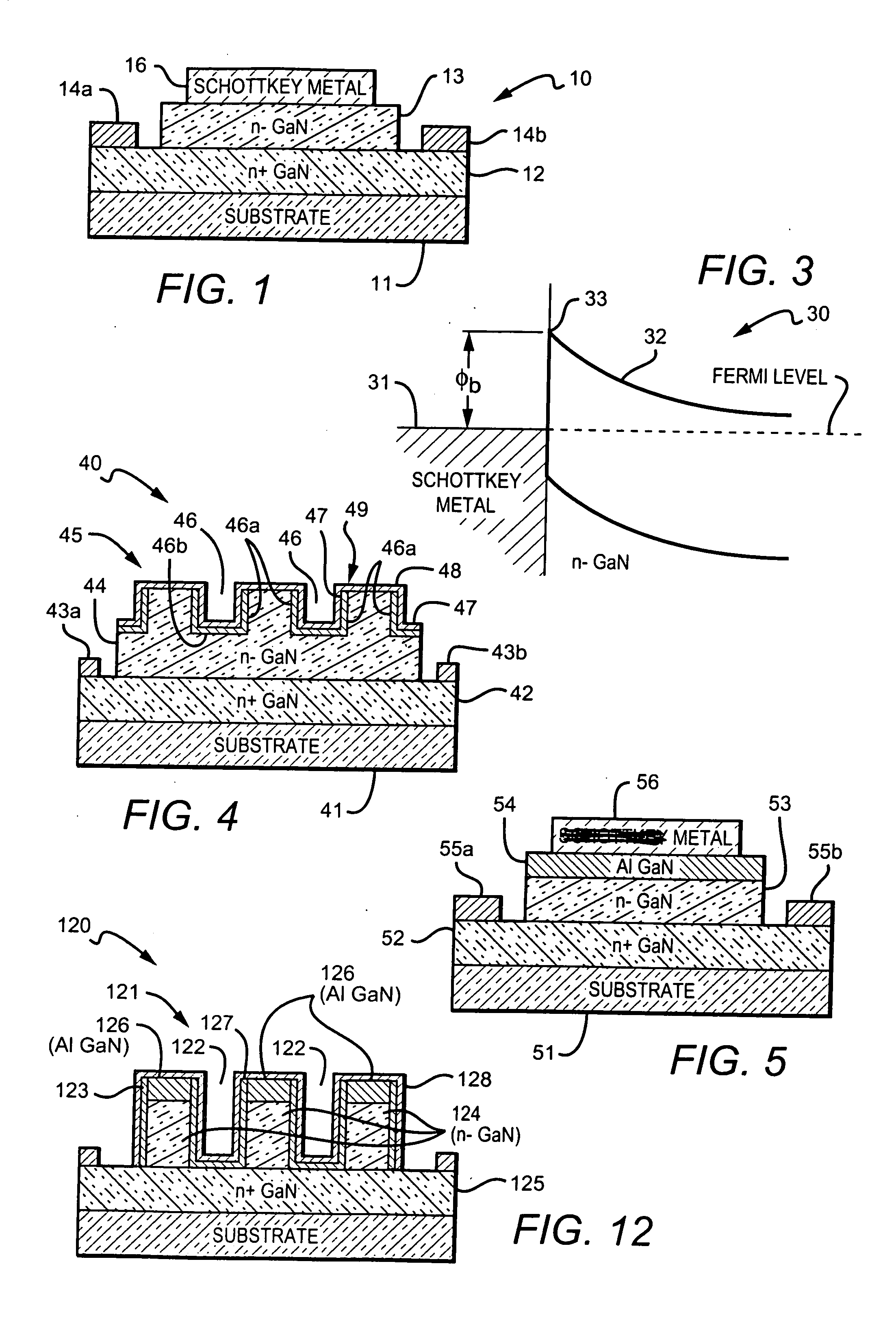
The present invention provides new Group III nitride based diodes with low Vf and low Irev. The new diodes have a unique structure that prevents an increase in Irev while maintaining low Vf. The diodes have a trench structure on their surface that prevents an increase in the electric field when the diode is under reverse bias. The trench structure includes parallel, equally spaced trenches with mesa regions between adjacent trenches. The trenches have an insulating layer on their sidewalls and bottom surface, and a continuous Schottky metal layer covering the insulating layer and the mesas between the trenches. The patent also describes a GaN tunnel diode with low Vf resulting from the tunneling of electrons through the barrier potential. The design of the barrier layer maximizes the forward tunneling probability and the different thickness and Al mole fraction of the barrier layer result in different forward and reverse operating characteristics.

Problems solved by technology

Using a metal that reduces the Schottky barrier potential results in a low Vf, but can also result in an undesirable increase in Irev.

Method used


Image

  • Gallium nitride based diodes with low forward voltage and low reverse current operation
  • Gallium nitride based diodes with low forward voltage and low reverse current operation
  • Gallium nitride based diodes with low forward voltage and low reverse current operation

Examples


Embodiment Construction

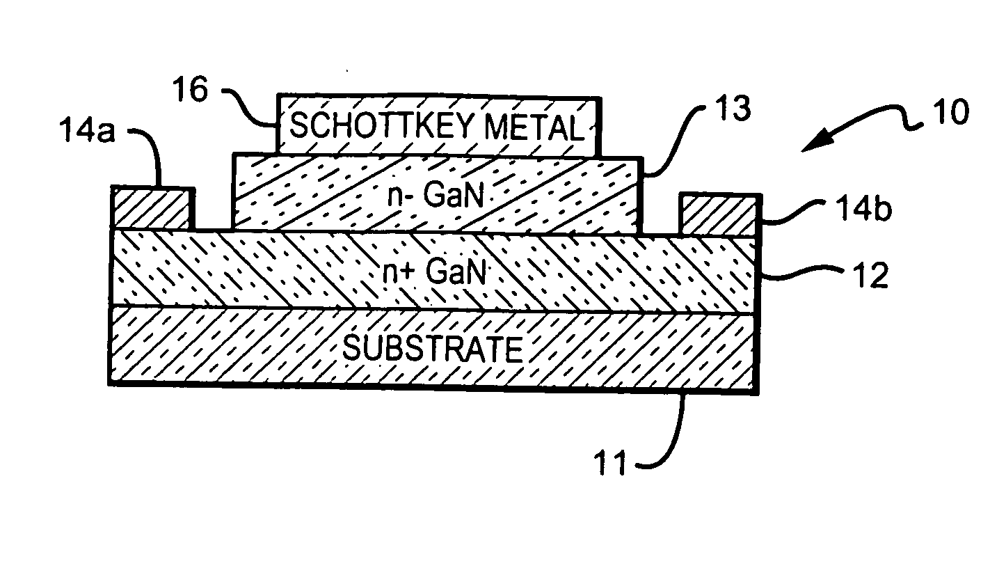
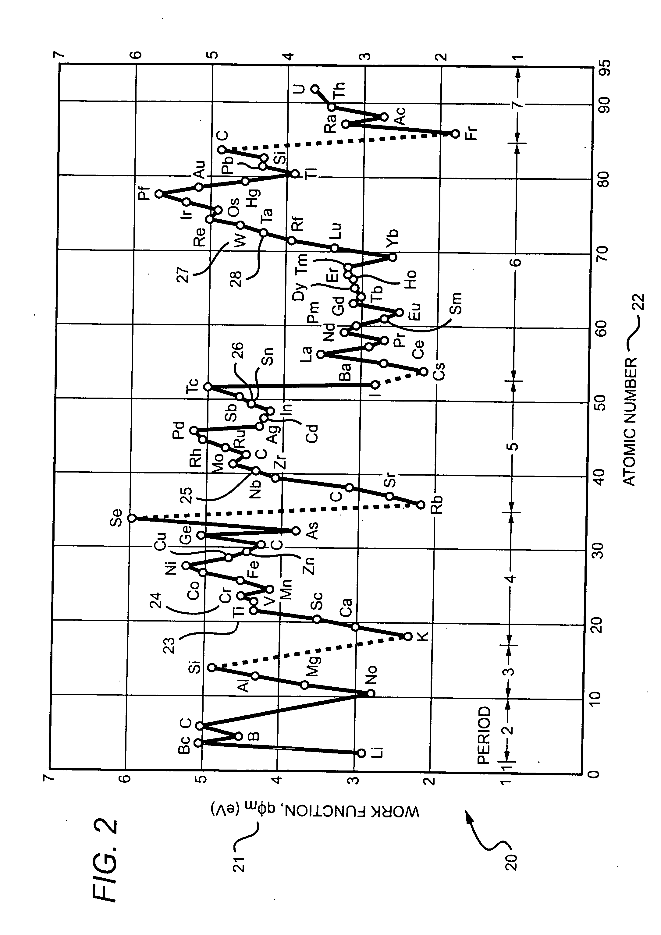
[0032]FIG. 1 shows a Schottky diode 10 constructed in accordance with the present invention having a reduced metal-to-semiconductor barrier potential. The new diode is formed of the Group III nitride based material system or other material systems where the Fermi level is not pinned at its surface states. Group III nitrides refer to those semiconductor compounds formed between nitrogen and the elements in Group III of the periodic table, usually aluminum (Al), gallium (Ga), and indium (In). The term also refers to ternary and tertiary compounds such as AlGaN and AlInGaN. The preferred materials for the new diode are GaN and AlGaN.

[0033] The new diode 10 comprises a substrate 11 that can be either sapphire (Al2O3), silicon (Si) or silicon carbide (SiC), with the preferred substrate being a 4H polytype of silicon carbide. Other silicon carbide polytypes can also be used including 3C, 6H and 15R polytypes. An AlxGa1-xN buffer layer 12 (where x in between 0 and 1) is included on the su...


PUM


Abstract

New Group III based diodes are disclosed having a low on state voltage (Vf) and structures to keep reverse current (Irev) relatively low. One embodiment of the invention is Schottky barrier diode made from the GaN material system in which the Fermi level (or surface potential) of is not pinned. The barrier potential at the metal-to-semiconductor junction varies depending on the type of metal used and using particular metals lowers the diode's Schottky barrier potential and results in a Vf in the range of 0.1-0.3V. In another embodiment a trench structure is formed on the Schottky diodes semiconductor material to reduce reverse leakage current. and comprises a number of parallel, equally spaced trenches with mesa regions between adjacent trenches. A third embodiment of the invention provides a GaN tunnel diode with a low Vf resulting from the tunneling of electrons through the barrier potential, instead of over it. This embodiment can also have a trench structure to reduce reverse leakage current.

Description

BACKGROUND OF THE INVENTION [0001] 1. Field of the Invention [0002] This invention relates to diodes, and more particularly to gallium nitride (GaN) based diodes exhibiting improved forward voltage and reverse leakage current characteristics. [0003] 2. Description of the Related Art [0004] Diode rectifiers are one of the most widely used devices for low voltage switching, power supplies, power converters and related applications. For efficient operation it is desirable for diodes to have low on-state voltage (0.1-0.2V or lower), low reverse leakage current, high voltage blocking capability (20-30V), and high switching speed. [0005] The most common diodes are pn-junction diodes made from silicon (Si) with impurity elements introduced to modify, in a controlled manner, the diode's operating characteristics. Diodes can also be formed from other semiconductor materials such as Gallium Arsenide (GaAs) and silicon carbide (SiC). One disadvantage of junction diodes is that during forward c...

Claims


Application Information

Patent Timeline
Patent Type & Authority Applications(United States)
IPC IPC(8): H01L29/20H01L29/22H01L29/47H01L29/872H01L29/88
CPCH01L29/2003H01L29/88H01L29/872H01L29/475H01L29/8725
Inventor PARIKH, PRIMITMISHRA, UMESH
Owner CREE INC
Learn More