

Carbon nanotube, electron emission source including the same, electron emission device including the electron emission source,and method of manufacturing the electron emission device
a carbon nanotube and emission source technology, applied in the field of carbon nanotubes, can solve the problems of not meeting the desired level of electron emission characteristics of the electron emission devices developed up to now, and achieve the effect of less defects and high reliability
Inactive Publication Date: 2005-11-03
SAMSUNG SDI CO LTD
View PDF6 Cites 35 Cited by
- Summary
- Abstract
- Description
- Claims
- Application Information
AI Technical Summary
Benefits of technology
[0009] It is therefore, an object of the present invention to provide a carbon nanotube (CNT) capable of improving electron emission capability, an electron emission source including the same, an electron emission device including the electron emission source, and a method of manufacturing the electron emission device.
[0011] It is yet another object of the present invention to provide CNT that has high reliability, where the CNT can be provided in an electron emitting source or in an electron emitting source provided in an electron emission device.
[0012] It is still another object of the present invention to provide a technique of manufacturing an electron emission device with CNT that has more defect-free carbon crystals than a conventional CNT and therefore a higher reliability that is easy to implement and cost effective while still being efficient.
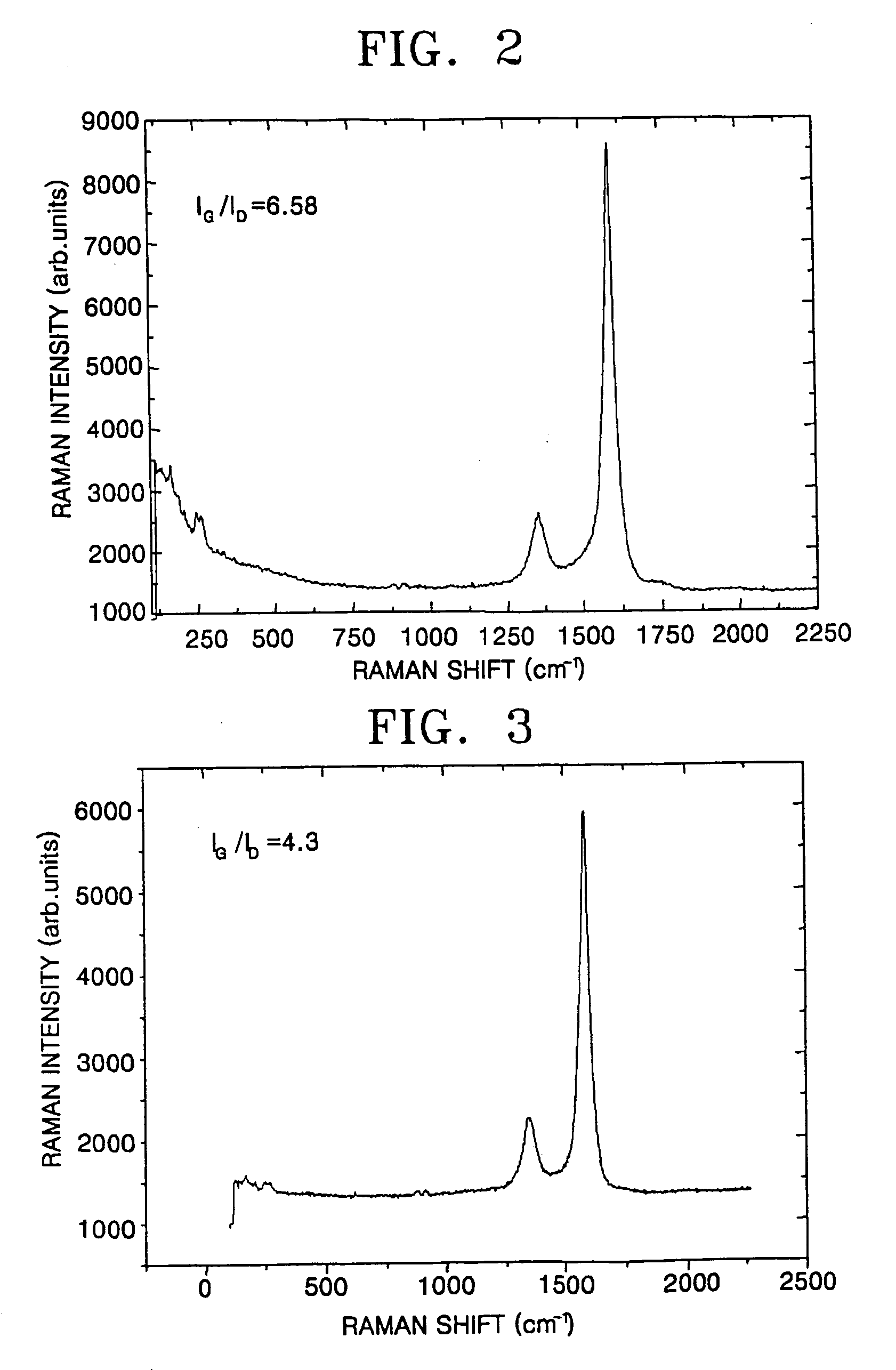
[0019] A CNT according to the present invention has Raman spectrum of the CNT having a G band and a D band, wherein the ratio of the G band peak integral (IG) to the D band peak integral (ID) is 5 or greater, thereby having less defects than conventional CNTs. As a result, an electron emission device including an electron emission source including the CNT is highly reliable.
Problems solved by technology
However, electron emission devices developed up to now, including the electron emission devices disclosed in the above-mentioned Patent, U.S. Pat. No. 6,608,437, have not met a desired level of electron emission characteristics.
Method used
View moreImage
Smart ImageViewing Examples

Examples
example 1
MEASUREMENT EXAMPLE 1
Current Density Measurement
[0072] Current densities of Sample 1 and Samples A and B were measured and the results are shown in FIG. 5. Referring to FIG. 5, the current density of Sample 1 at 5V / um was 400 μA / cm2, and the current density of Samples A and B were about 50 μA / cm2. The current density plot of Sample 1 was confirmed to have much larger gradient than that of Samples A and B.
Login to View More PUM
| Property | Measurement | Unit |
|---|---|---|
| Raman shift | aaaaa | aaaaa |
| Raman shift | aaaaa | aaaaa |
| current density | aaaaa | aaaaa |
Abstract
A carbon nanotube (CNT) with Raman spectrum having a G band and a D band, includes a ratio of a G band peak integral IG and a D band peak integral ID is 5 or greater. Further, there is an electron emission source including the CNT, an electron emission device including the electron emission source and a method of manufacturing the electron emission device. The electron emission source including the CNT has preferred current density, so the electron emission device using the electron emission source is highly reliable.
Description
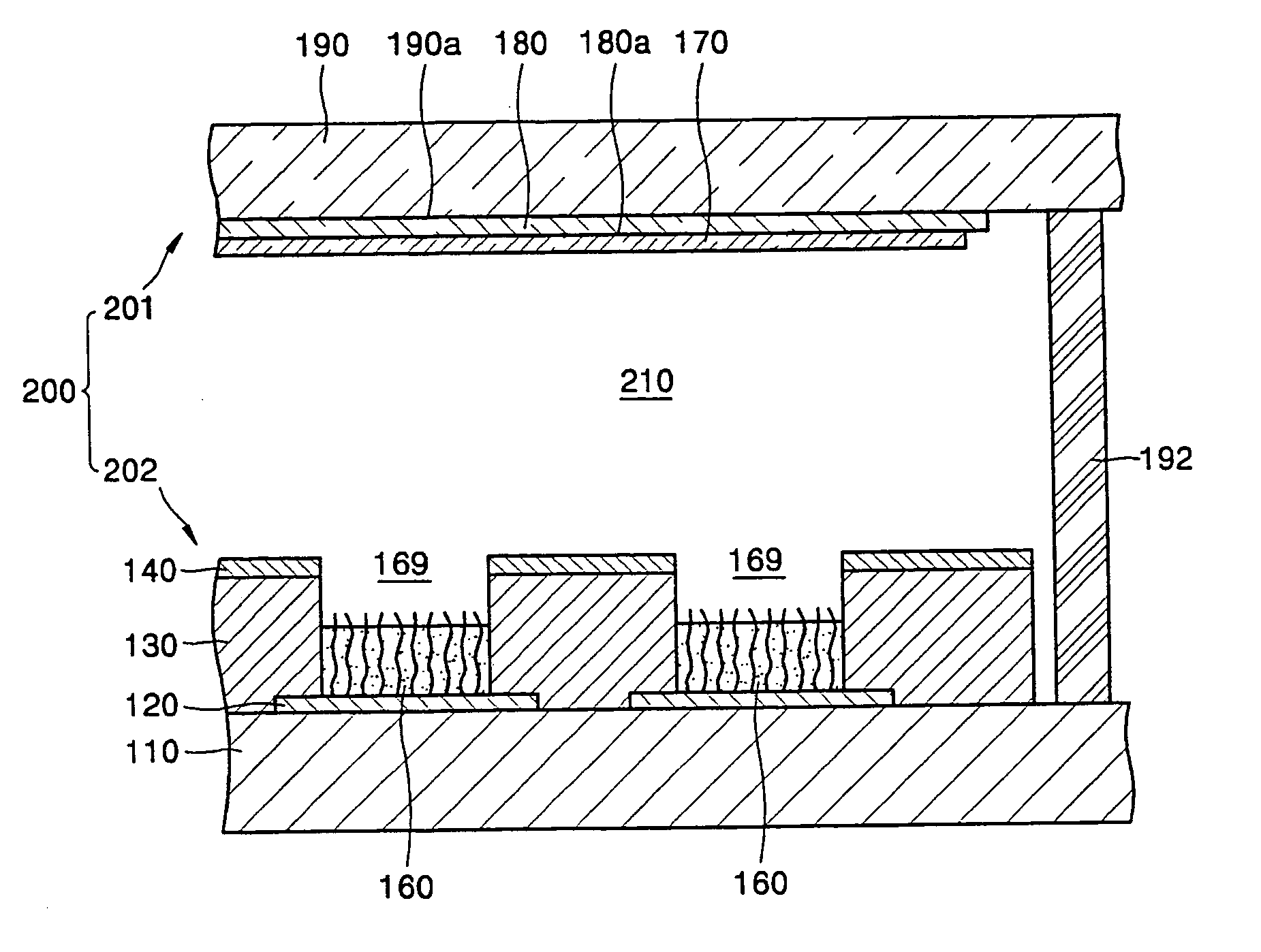
CLAIM OF PRIORITY [0001] This application makes reference to, incorporates the same herein, and claims all benefits accruing under 35 U.S.C. § 119 from an application for A CARBON NANOTUBE, AN EMITTER COMPRISING THE CARBON NANOTUBE AND AN ELECTRON EMISSION DEVICE COMPRISING THE EMITTER earlier filed in the Korean Intellectual Property Office on 29 Apr. 2004 and there duly assigned Serial No. 10-2004-0030258. BACKGROUND OF THE INVENTION [0002] 1. Field of the Invention [0003] The present invention relates to a CNT (carbon nanotube), an electron emission source including the same, an electron emission device including the electron emission source, and a method of manufacturing the electron emission device, and more particularly, to a CNT with Raman spectrum having a G band and a D band, wherein a ratio of a G band peak integral (IG) to a D band peak integral (ID) is 5 or greater, an electron emission source including the CNT, an electron emission device including the electron emission...
Claims
Login to View More Application Information
Patent Timeline
 Patent Type & AuthorityApplications(United States)
IPC IPC(8): C01B31/02H01J1/30H01J1/304H01J9/02H01L29/06H10K99/00
CPCB82Y10/00H01J1/3044H01L51/0052H01L51/0048H01J2201/30469H10K85/221H10K85/615
InventorNAM, JOONG-WOOPARK, JONG-HWANRYU, MEE-AE
OwnerSAMSUNG SDI CO LTD