Film formation apparatus and method of using the same

a technology of film formation apparatus and film, which is applied in the field of film formation apparatus and the use of the same, can solve the problems of reducing the yield of semiconductor devices to be manufactured, deteriorating internal parts of the apparatus, and so as to achieve the effect of increasing the downtime of the apparatus

Active Publication Date: 2005-11-03
TOKYO ELECTRON LTD
View PDF2 Cites 12 Cited by
  • Summary
  • Abstract
  • Description
  • Claims
  • Application Information

AI Technical Summary

Benefits of technology

[0010] An object of the present invention is to provide a film formation apparatus for a semiconductor process and a method of using the same, which can prevent internal parts of the apparatus from being deteriorated, and downtime of the apparatus from being increased.

Problems solved by technology

The particles may drop onto the semiconductor wafer, and reduce the yield of semiconductor devices to be fabricated.
However, as described later, the present inventors have found that conventional cleaning methods of this kind may cause problems in that internal parts of the apparatus are deteriorated, or downtime of the apparatus is increased.

Method used


Image

  • Film formation apparatus and method of using the same
  • Film formation apparatus and method of using the same
  • Film formation apparatus and method of using the same

Examples


Embodiment Construction

[0031] In the process of developing the present invention, the inventors studied problems with regard to conventional methods for cleaning the interior of a reaction tube used in a film formation apparatus for a semiconductor process. As a result, the inventors have arrived at the findings given below.

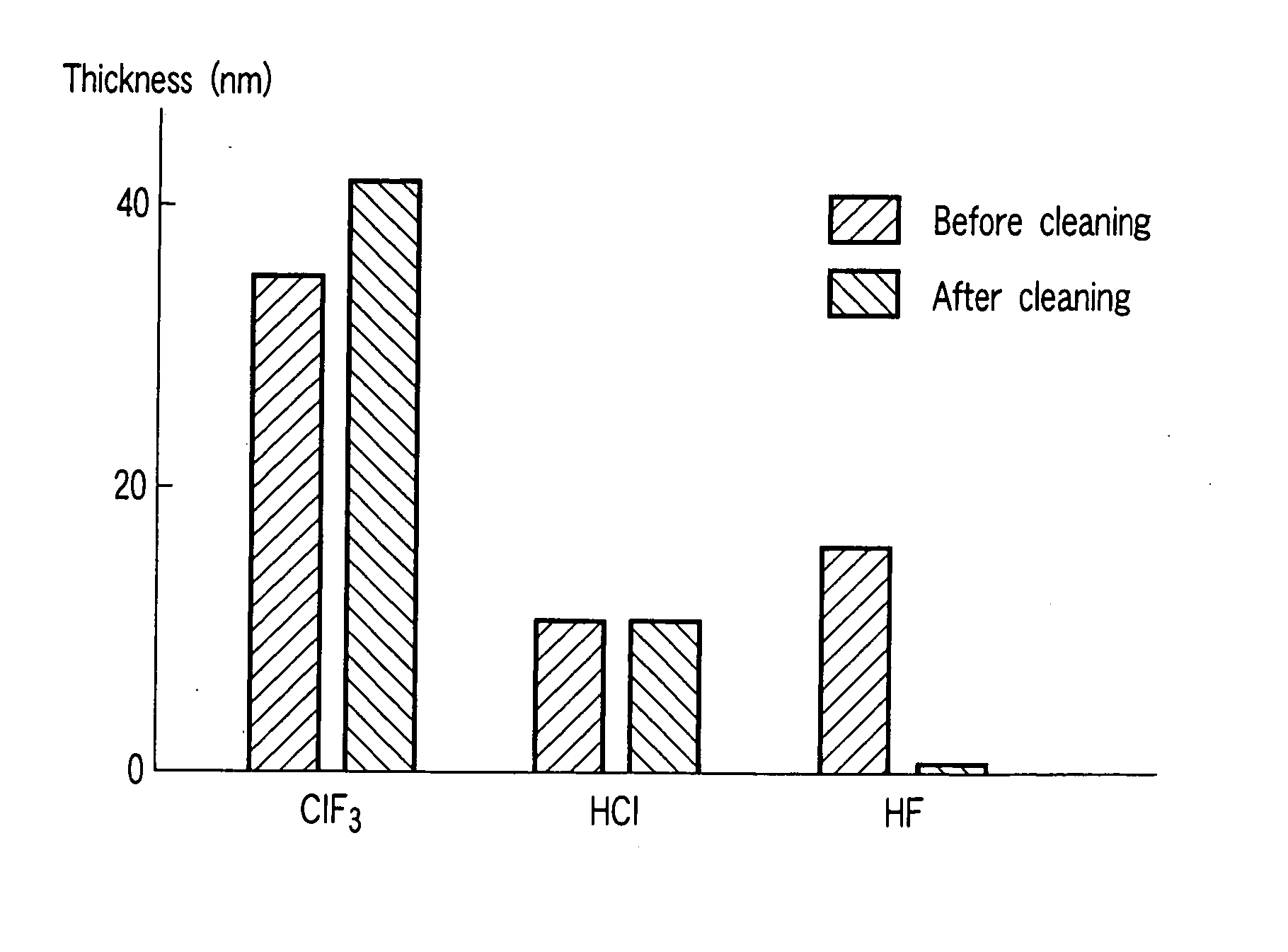
[0032] Specifically, in order to remove by-product films deposited inside a reaction tube while supplying a cleaning gas, it is necessary to heat up the interior of the reaction tube. For example, where a by-product film consists of a compound with a low vapor pressure, the interior of the reaction tube needs to be heated up to a high temperature, so that the compound can be allocated with a sufficiently high vapor pressure. However, when a cleaning gas is supplied into the reaction tube heated at a high temperature, the material of the reaction tube, such as quartz, is damaged, thereby shortening the service life of the reaction tube. Further, corrosion of metal members used for an e...


PUM

PropertyMeasurementUnit
temperatureaaaaaaaaaa
pressureaaaaaaaaaa
temperatureaaaaaaaaaa

Abstract

A method of using a film formation apparatus for a semiconductor process includes a step of removing a by-product film deposited on an inner surface of a reaction chamber of the film formation apparatus. This step is performed while supplying a cleaning gas containing hydrogen fluoride into the reaction chamber, and forming a first atmosphere within the reaction chamber, which allows water to be present as a liquid film.

Description

CROSS-REFERENCE TO RELATED APPLICATIONS [0001] This application is based upon and claims the benefit of priority from prior Japanese Patent Applications No. 2004-127570, filed Apr. 23, 2004; and No. 2005-075048, filed Mar. 16, 2005, the entire contents of both of which are incorporated herein by reference. BACKGROUND OF THE INVENTION [0002] 1. Field of the Invention [0003] The present invention relates to a film formation apparatus for a semiconductor process for forming a film on a target substrate, such as a semiconductor wafer, and also to a method of using the apparatus. The term “semiconductor process” used herein includes various kinds of processes which are performed to manufacture a semiconductor device or a structure having wiring layers, electrodes, and the like to be connected to a semiconductor device, on a target substrate, such as a semiconductor wafer or a glass substrate used for an LCD (Liquid Crystal Display) or FPD (Flat Panel Display), by forming semiconductor la...

Claims


Application Information

Patent Timeline
Patent Type & Authority Applications(United States)
IPC IPC(8): B08B7/00B08B7/04B08B5/00C23C16/00C23C16/44H01L21/304H01L21/3065H01L21/31H01L21/469
CPCB08B7/0035Y10S438/90C23C16/4405A47G1/02A47G1/10A47B67/005
Inventor ENDO, ATSUSHIFUJIWARA, TOMONORIMOROZUMI, YUICHIROHARADA, KATSUSHIGENAKAJIMA, SHIGERUCHOI, DONG-KYUNFURUYA, HARUHIKOYABE, KAZUO
Owner TOKYO ELECTRON LTD
Why Eureka
Try Eureka