Light-emitting apparatus
a technology of light-emitting apparatus and light-emitting electrode, which is applied in the direction of electroluminescent light sources, semiconductor devices, basic electric elements, etc., can solve the problems of poor coverage, short-circuiting of the second electrode, and restricted opening ratio, so as to improve the opening ratio and light extraction efficiency, reduce defects, and reduce defects
- Summary
- Abstract
- Description
- Claims
- Application Information
AI Technical Summary
Benefits of technology
Problems solved by technology
Method used
Image
Examples
example 1
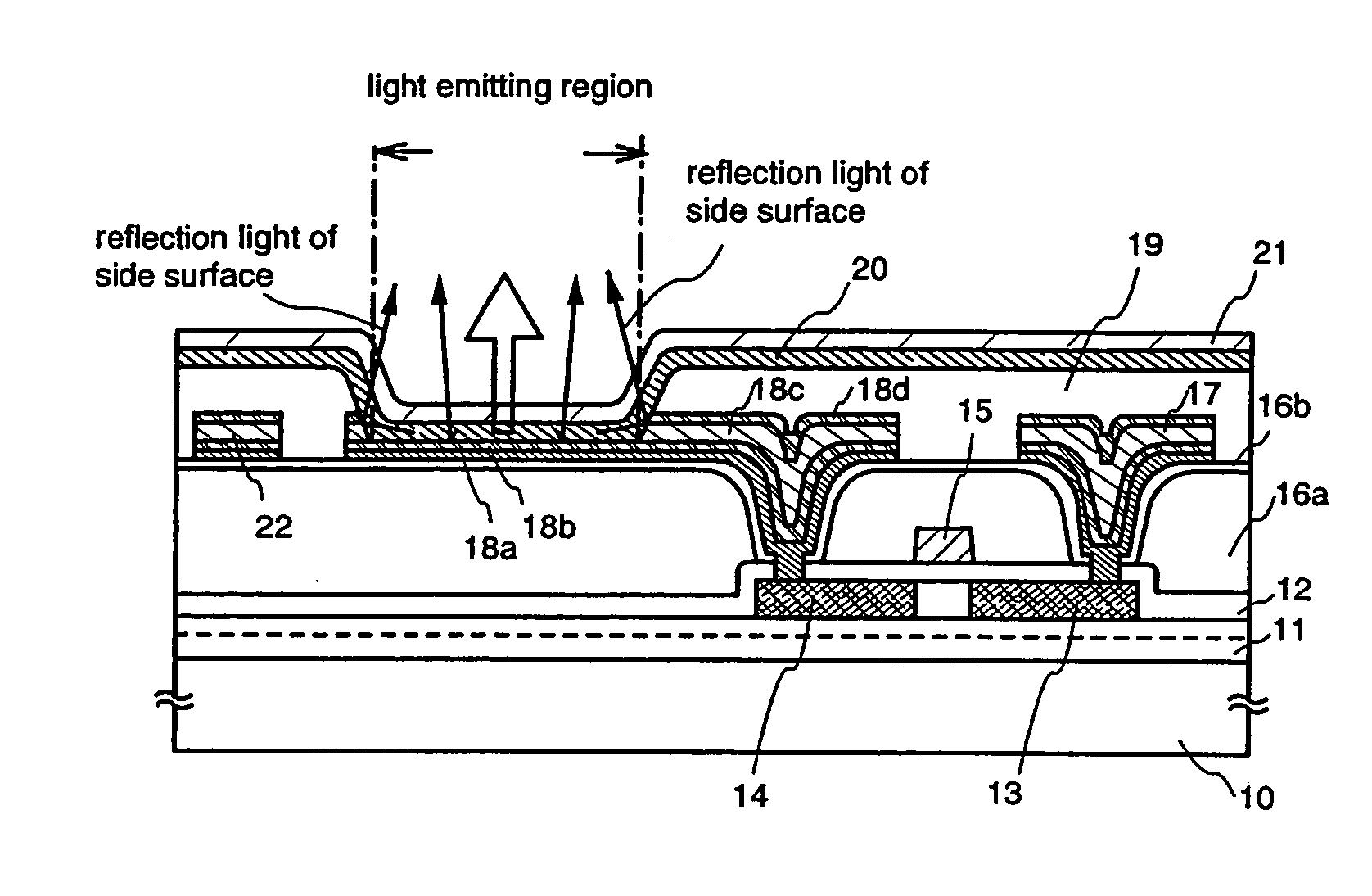
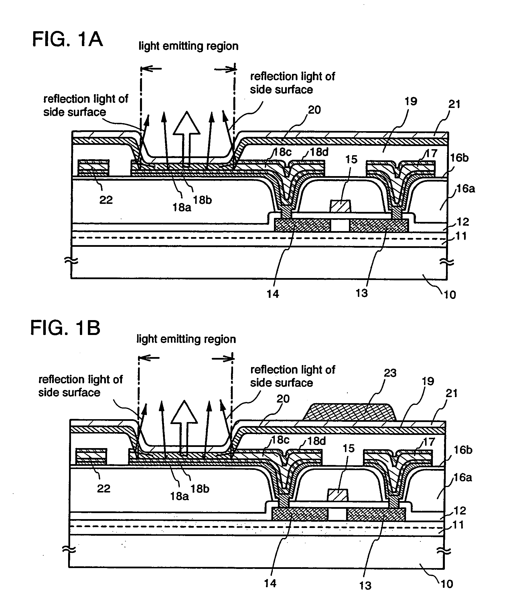
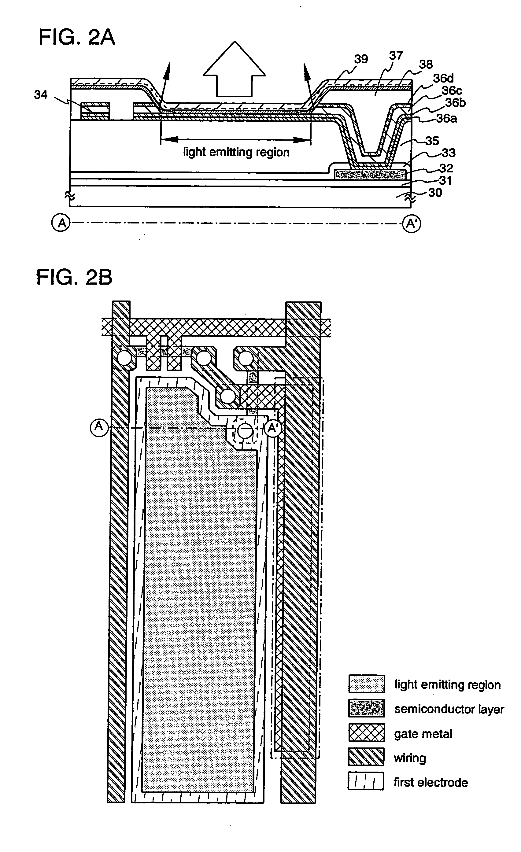
[0077] Hereinafter, a brief description of an example of procedure of forming a light-emitting device in accordance with the present invention is explained with reference to FIGS. 2A to 3C in this example.
[0078] First, a base insulating film 31 is deposited over a substrate 30 which has an insulating surface.
[0079] A silicon oxynitride film is deposited as the first layer of the base insulating film to have a thickness of from 10 to 200 nm (preferably, from 50 to 100 nm) by plasma CVD using reaction gas of SiH4, NH3, and N2O. Here, a silicon oxynitride film (composition ratio: Si=32%, O=27%, N=24%, H=17%) with a thickness of 50 nm is deposited. A silicon oxynitride film is deposited as the second layer of the base insulating film to have a thickness of form 50 to 200 nm (preferably, from 100 to 150 nm) by plasma CVD using as reaction gas of SiH4 and N2O. Here, a silicon oxynitride film (composition ratio: Si=32%, O=59%, N=7%, H=2%) with a thickness of 100 nm is formed. The base in...
example 2
[0102] The state of a residue generated due to etching for forming steps of a first electrode will be described with reference to experimental results. As shown in FIGS. 4A and 4B, the first electrode is classified broadly into type 1 (Without a fourth layer) and type 2 (with a fourth layer) by the state of lamination, respectively. The state of an etched third layer that is formed of another material is observed. The first and the second layers are formed of common materials, the first layer is formed of Ti, and the second layer is formed of TiN. In case of forming the fourth layer, Ti is used for forming the fourth layer. The fourth layer is formed of Ti in this example, but can also be formed of TiN.
[0103] The sample that is used for observing an etching residue is made by forming silicon nitride over a glass substrate and forming a quasi electrode having a lamination structure that serves as the first electrode. A metal film that serves as the first to the fourth layers is form...
example 3
[0113] Observation using an atomic force microscope (AFM) is carried out to the TiN surface state of a quasi electrode sample (state 1: Ti / TiN / Al—Ti / Ti) without a residue, of which the inclined plane is formed by adopting the lamination structure according to the present invention; and the TiN surface state of a quasi electrode sample (state 2: Ti / TiN / Al—Si / Ti) with residue, which is not formed by adopting the lamination structure according to the present invention. The cross-sectional surfaces of the sample of state 1 and the sample of state 2 are observed to obtain the radius of curvature of irregularities by transmission electron microscope (TEM). A portion having small radius of curvature that may have an effect on light emission of an organic light-emitting layer is particularly measured since a portion having large radius of curvature is nearly a flat surface.
[0114] An aspect ratio of irregularities is obtained by height and distance between a peak and an adjacent valley in a...
PUM
 Abstract
Description
Claims
Application Information


