

Electronic device with high lead density
- Summary
- Abstract
- Description
- Claims
- Application Information
AI Technical Summary
Benefits of technology
Problems solved by technology
Method used
Image

Examples
Embodiment Construction
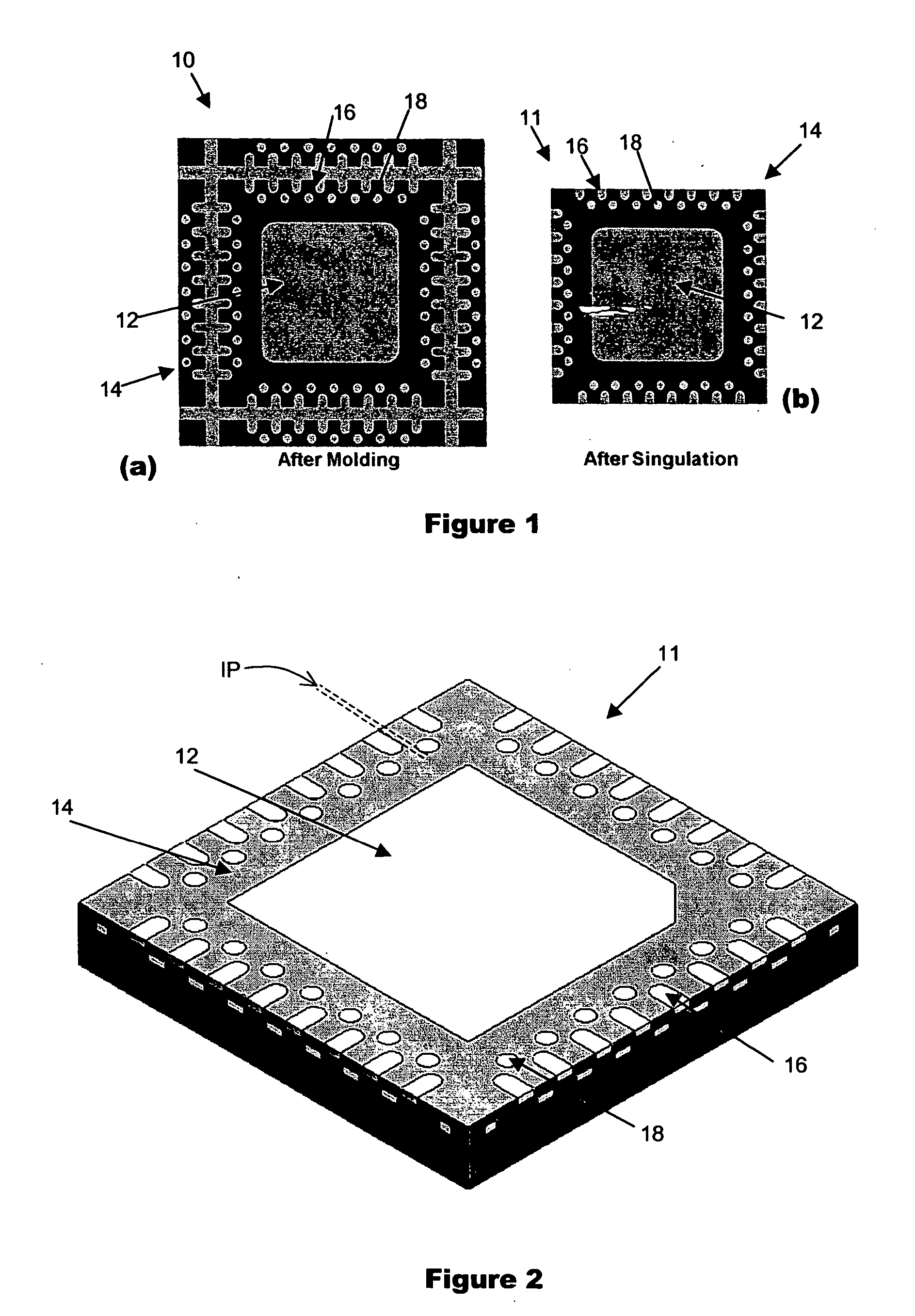
[0021]FIG. 1(a) illustrates a plan view of a molded leadless QFN semiconductor package 10 after molding. The view shows a bottom side of the leadless package with exposed electrical contacts. It shows a base of a die pad 12 to which an integrated circuit die has been attached to a top side, areas covered by a molding compound 14, outer leads 16 and inner leads 18.
[0022]FIG. 1(b) illustrates a plan view of the leadless molded package 11 after singulation. An outer peripheral of the package 11 has been diced adjacent to the position of the outer leads 16 so as to leave a sufficient surface area remaining of the outer leads 16 and inner leads 18 for contact with a mounting surface.
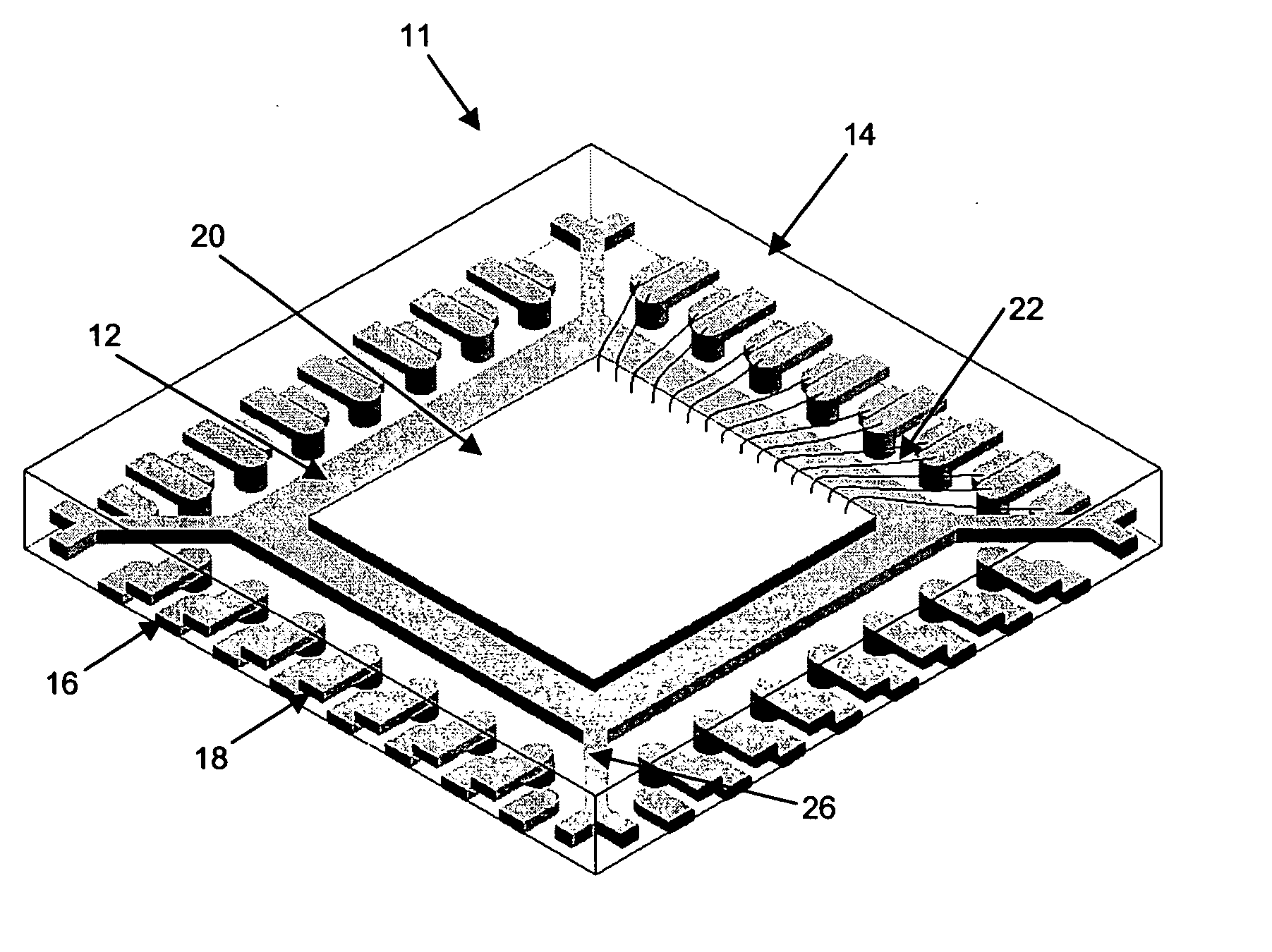
[0023]FIG. 2 illustrates an isometric view of the molded package after singulation. An internal pitch (“IP”) of leads of the QFN package 11 is shown, which refers to a distance between adjacent contact leads to which bonding wires may be connected. In the preferred embodiment of the invention, the leads com...
PUM
 Abstract
Description
Claims
Application Information