Over-passivation process of forming polymer layer over IC chip

a technology of ic chip and polymer layer, which is applied in the direction of semiconductor devices, semiconductor/solid-state device details, electrical equipment, etc., can solve the problems of increasing production costs, affecting the quality of electrical signal passing through, and affecting the mechanical integrity of the jointing structure, so as to reduce the occurrence of inter-metallic compounds

Inactive Publication Date: 2005-11-10
QUALCOMM INC
View PDF4 Cites 28 Cited by
  • Summary
  • Abstract
  • Description
  • Claims
  • Application Information

AI Technical Summary

Benefits of technology

[0038] In summary, the invented over-passivation process uses a temperature below 320° C. to cure the patterned polymer layer. Thus, it can reduce the occurrence of the inter-metallic compound. The other advantage of the invented over-passivation process lies on the alleviation of the thermal budget of the entire IC manufacturing process, which in turn helps solve other problems caused by high temperature process.

Problems solved by technology

It should be noted that the aluminum-gold inter-metallic compound 180 is a porous structure; it not only weakens the mechanical integrity of the jointing structure, but also deteriorates the quality of electrical signal passing therethrough.
Regardless of which of the above process used, they both will increase the cost of production.
Also, the quality of the electrical signal passing therethrough will be deteriorated in that a thickened or doped barrier layer 150 increases its parasitic resistance.
The other disadvantage of the high temperature curing process of polyimide layers lies on its impact on the thermal budget of IC manufacturing process.
Because traditional curing process of polyimide layer is run at high temperature for several hours, and there may be multiple polyimide layers deposited over the semiconductor wafer, the curing process of polyimide will inevitably suppress the whole thermal budget to manufacture the semiconductor wafer 100.
It is the trend of today's semiconductor fabrication process to lower the thermal budget since high temperature processes usually cause problems on the issues such as the formation of inter-metallic compound, diffusion among different layers, and exceeded thermal stress caused by the different thermal expansion coefficient of materials, etc.
The resulted expansion of the doped region may cause the side effect of gate channel shortening or the concentration profile change of the doped area.

Method used


Image

  • Over-passivation process of forming polymer layer over IC chip
  • Over-passivation process of forming polymer layer over IC chip
  • Over-passivation process of forming polymer layer over IC chip

Examples


first embodiment

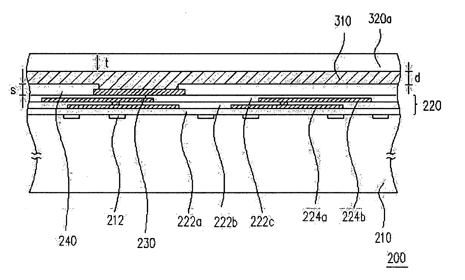
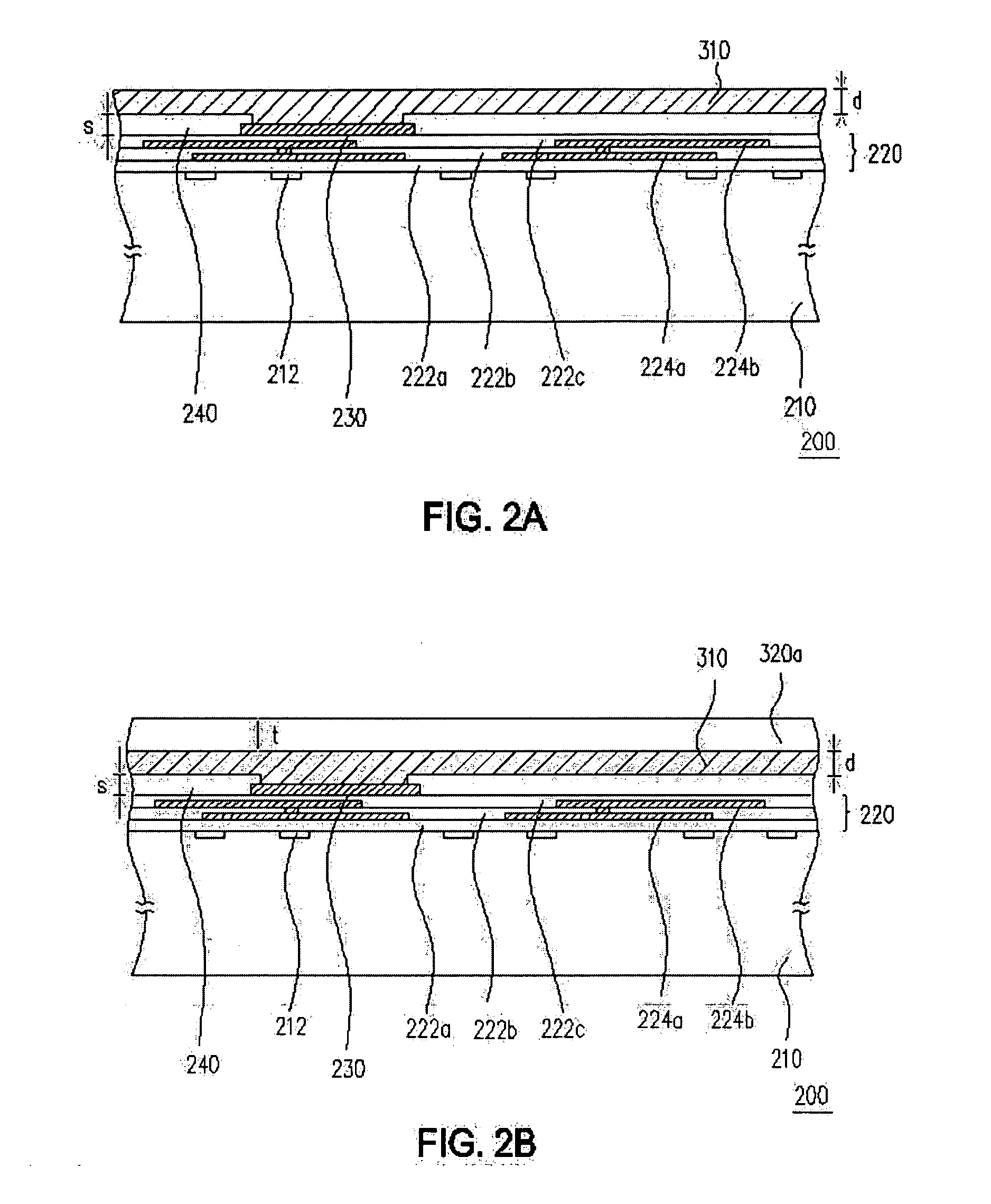
[0046]FIGS. 2A through 2C are cross-sectional representations of a over-passivation process of first preferred embodiment of the present invention. As shown in FIG. 2A, the over-passivation process comprises the following steps. First, a semiconductor wafer 200 is provided, wherein the semiconductor wafer 200 comprises a silicon substrate 210, an interconnection structure 220, a connection pad 230, and a passivation layer 240. The silicon substrate 210 has multiple active semiconductor devices composed of either transistors or MOS transistors, or both, even plus passive devices. Multiple electronic devices formed in or on the silicon substrate can be, for example, bipolar transistors, MOS transistors or passive devices. The electronic devices are the sub-micron devices, such as 0.18 micron, 0.13 micron or 0.11 micron CMOS devices, or sub-hundred-nanometer devices, such as 90 nanometer, 65 nanometer or 35 nanometer devices. The electronic devices 212 are placed in and on the the sili...

second embodiment

[0065]FIG. 4 is the cross-sectional representation of the over-passivation process of the second preferred embodiment of present invention. Some reference numbers appearing on the second embodiment are the same as those of the first preferred embodiment; in such case it means the elements referred by both embodiments are the same or similar.

[0066] In the second preferred embodiment, a patterned polymer layer 410 is first formed on the passivation layer 240, and a patterned metal circuit layer 420 is subsequently formed over the patterned polymer layer 410. More specifically, the step of forming the patterned polymer layer 410, as is briefly depicted above, comprises first forming an imide-oligomer layer, precursor layer, over the passivation layer 240; followed by curing. The polyimide is cured with a temperature cycle by heating the imide-oligomer layer upto a peak temperature between 200° C. and 320° C., and staying at about peak temperature for more than 20 minutes. The peak tem...

third embodiment

[0068]FIG. 4 is the cross-sectional representation of the over-passivation process of the second preferred embodiment of present invention. Some reference numbers appearing on the second embodiment are the same as those of the first preferred embodiment; in such case it means the elements referred by both embodiments are the same or similar.

[0069]FIGS. 5A and 5B are the cross-sectional representations of a over-passivation structure of a third preferred embodiment of the present invention. Some reference numbers appearing on the third embodiment are the same as those of the first preferred embodiment; in such a case it means the elements referred by both embodiments are the same or similar.

[0070] Referring to FIG. 5A, the over-passivation process comprises the following steps. First, a chip 200 is provided. Then a patterned metal circuit 510 is formed on the passivation layer 240. Hereafter a patterned polymer layer 520 is formed on the patterned metal circuit 510; the material us...


PUM

PropertyMeasurementUnit
peak temperatureaaaaaaaaaa
temperatureaaaaaaaaaa

Abstract

A method for forming a semiconductor chip or wafer includes following steps. A semiconductor substrate is provided, and then a polymer layer is deposited over the semiconductor substrate, wherein the polymer layer comprises polyimide. The polymer layer with a temperature profile having a peak temperature between 200 and 320 degrees Celsius. Alternatively, the temperature profile may comprises a period of time with a temperature higher than 320 degree Celsius, wherein the period of time is shorter than 45 minutes.

Description

[0001] This application is a continuation-in-part of application Ser. No. 10 / 154,662 filed on May 24, 2002, which is a continuation-in-part of application Ser. No. 10 / 058,259, filed on Jan. 29, 2002, now U.S. Pat. No. 6,660,728, which is a continuation of application Ser. No. 09 / 251,183, filed on Feb. 17, 1999, now U.S. Pat. No. 6,383,916, which is a continuation-in-part of application Ser. No. 09 / 216,791, filed on Dec. 21, 1998, now abandoned. This application is also a continuation-in-part of application Ser. No. 10 / 685,872, filed on Oct. 15, 2003, which is a continuation-in-part of application Ser. No. 10 / 287,106, filed on Oct. 22, 2002, now U.S. Pat. No. 6,734,563, which is a division of application Ser. No. 09 / 691,497, filed on Oct. 18, 2000, now U.S. Pat. No. 6,495,442. This application is a continuation-in-part of application Ser. No. 10 / 710,596, filed on Jul. 23, 2004, which is a continuation-in-part of application Ser. No. 10 / 445,558, filed on May 27, 2003, which is a conti...

Claims


Application Information

Patent Timeline
Patent Type & Authority Applications(United States)
IPC IPC(8): H01L21/00H01L21/312H01L23/29H01L23/31H01L23/525
CPCH01L21/312H01L23/293H01L23/3114H01L23/525H01L2924/0002H01L2924/12044H01L2924/00H01L21/02118H01L21/02337
Inventor CHEN, YING-CHIH
Owner QUALCOMM INC
Why Eureka
Try Eureka