Fabrication method of semiconductor integrated circuit device

Inactive Publication Date: 2005-11-10
RENESAS ELECTRONICS CORP
View PDF21 Cites 12 Cited by
  • Summary
  • Abstract
  • Description
  • Claims
  • Application Information

AI Technical Summary

Benefits of technology

[0004] For decreasing the resistivity of wirings that constitute a semiconductor integrated circuit device, the application of a damascene method using copper series materials (copper or copper alloys) for wiring materials have been developed. The damascene method comprises the steps of forming grooves to accommodate wirings in an insulative film, then depositing a conductor film for forming the wirings on the insulation film and in the grooves for forming the

Problems solved by technology

This method can decrease the size of the wirings compared with the size of the wirings of usual structures and, more particularly, reduce the fabrication s

Method used


Image

  • Fabrication method of semiconductor integrated circuit device
  • Fabrication method of semiconductor integrated circuit device
  • Fabrication method of semiconductor integrated circuit device

Examples


embodiment 1

[0080] In Embodiment 1, this embodiment of the invention is applied, for example, to a method of fabrication of a semiconductor integrated circuit device in which an nMISQn is formed in a p-well in a semiconductor substrate.

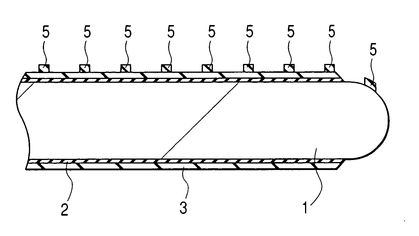
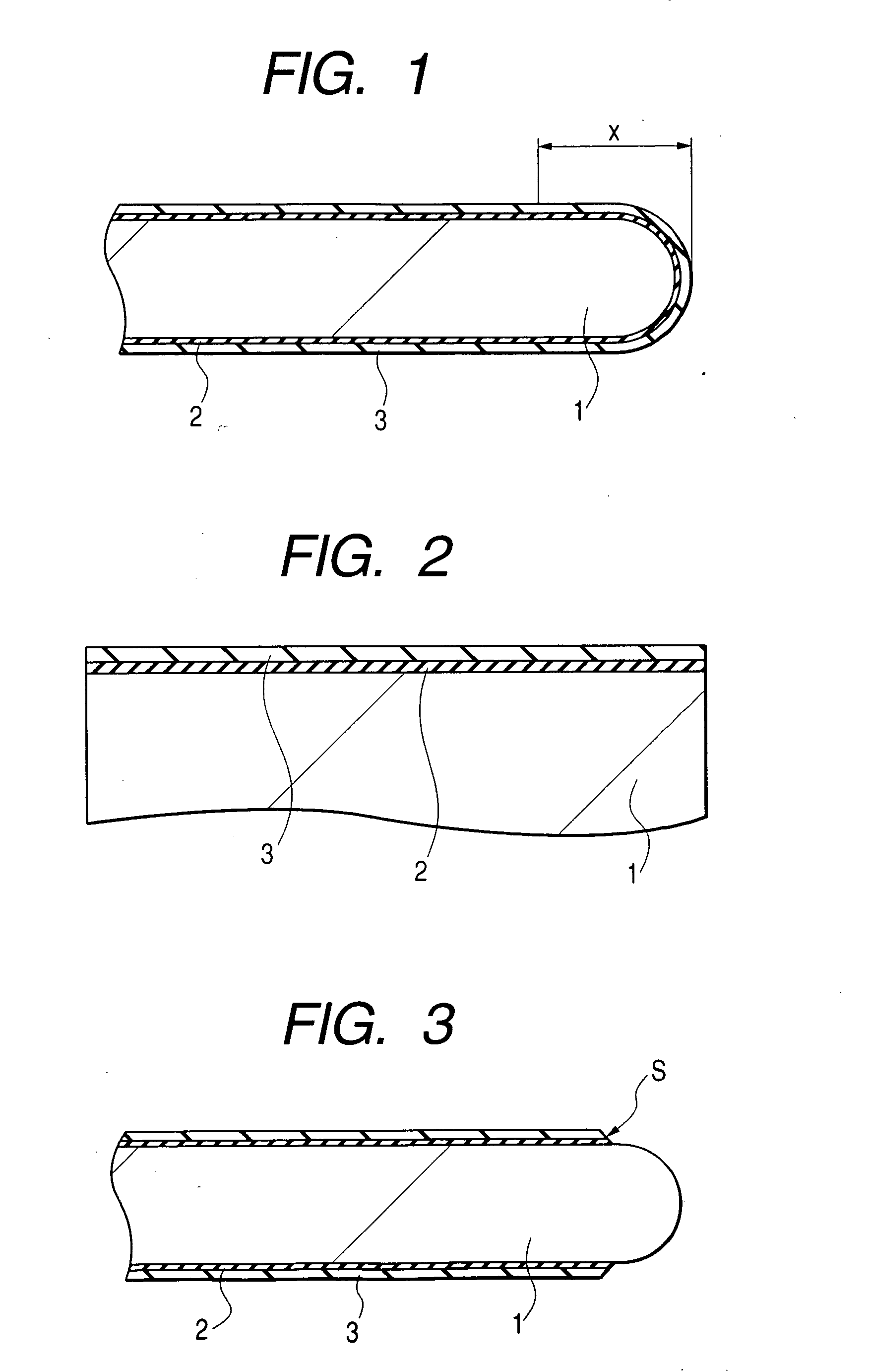
[0081]FIG. 1 and FIG. 2 are fragmentary cross sectional views of a wafer (semiconductor substrate) 1 of Embodiment 1. FIG. 1 shows, particularly, the vicinity of an edge of the wafer 1, and FIG. 2 shows, particularly, the vicinity of a device forming surface in the wafer 1 on an enlarged scale.

[0082] At first, as shown in FIG. 1 and FIG. 2, a wafer comprising a single crystal silicon (semiconductor substrate) 1 having a specific resistivity of about 10 Ωcm is provided. FIG. 2 is a fragmentary cross sectional view showing, on an enlarged scale, the vicinity of a device surface of the wafer 1. In Embodiment 1, the wafer has a thickness of about 750 μm and an outer periphery in a rounded state of about 350 μm radius. Further, in Embodiment 1, the edge width X of t...

embodiment 2

[0129] In Embodiment 2, thin films to be removed on the edge of the wafer are patterned before the removing step. Other components and fabrication steps are identical to those of Embodiment 1 as described above.

[0130] The method of fabrication of the semiconductor integrated circuit device of Embodiment 2 includes the same steps up to those that have been explained for Embodiment 1 with reference to FIG. 1 and FIG. 2.

[0131] Then, as shown in FIG. 36, after coating the photoresist film 5 above the wafer 1, the photoresist film 5 is patterned by exposure using a mask. Successively, as shown in FIG. 37, the silicon nitride film 3 and the silicon oxide film 2 in the device isolation regions are removed by dry etching using the photoresist film 5 as a mask. Successively, grooves 6, each of about 350 nm depth, are formed above the wafer 1 in the device isolation region by dry etching using the silicon nitride films 3 as a mask.

[0132] Then, as shown in FIG. 38, the wafer 1 is heat treat...

embodiment 3

[0138] In the method of fabrication of a semiconductor integrated circuit device according to Embodiment 3, this invention is applied to a semiconductor integrated circuit device having wirings, for example, formed of Al (aluminum) or aluminum alloy.

[0139] The method of fabrication of the semiconductor integrated circuit device of Embodiment 3 includes the same steps as those explained with reference to FIG. 1 to FIG. 25 for Embodiment 1.

[0140] Subsequently, as shown in FIG. 44 and FIG. 45, a conductive film 22C (first conductive film), such as TiN, is deposited above the wafer 1 by a sputtering method. In FIG. 44, the conductive film 22C is not illustrated to provide easy understanding of the step for forming wirings on the silicon oxide film 16.

[0141] Successively, a conductive film 22D, for example, made of Al (first conductive film) is deposited on the surface of the conductive film 22C. Further, successively, a conductive film 22E, for example, made of TiN is deposited on th...


PUM


Abstract

A method of fabrication of a semiconductor integrated circuit device, including polishing the entire area of an edge of a wafer, for example, uses three polishing drums in which a polishing drum polishes the upper surface of the edge of the wafer, a polishing drum polishes the central portion of the edge of the wafer and a polishing drum polishes the lower surface of the edge of the wafer, thereby preventing occurrence of obstacles which cause defoliation of thin films on the edge of the wafer.

Description

BACKGROUND OF THE INVENTION [0001] This invention concerns a method of fabrication of a semiconductor integrated circuit device; and, more particularly, it relates to a technique that is applicable to the fabrication of a semiconductor integrated circuit device, including fabrication of semiconductor wafers. [0002] The present inventors have conducted a search of the prior art with a view toward preventing the occurrence of obstacles extending from the edges of wafers. For example, Japanese Published Unexamined Patent Application No. 2000-68273 discloses a technique which involves polishing a metal film by a CMP method to form a pattern, and then removing any of the metal film which remains on edges of a device forming surface of the wafer by a wet etching method, laser or CMP method, thereby preventing the occurrence of obstacles extending from the edges. [0003] Further, polishing apparatuses for polishing the edges of wafers are disclosed, for example, in Japanese Published Unexam...

Claims


Application Information

Patent Timeline
IPC IPC(8): H01L21/304H01L21/3105H01L21/3205H01L21/321H01L21/76H01L21/768
CPCH01L21/0206H01L21/02068H01L21/3105H01L21/321H01L21/7685H01L21/76819H01L21/76838H01L21/7684H01L21/76843H01L21/76807H01L21/304
Inventor ARAI, TOSHIYUKIKAWAI, RYOUSEITSUCHIYAMA, HIROFUMIKANAI, FUMIYUKINAKABAYASHI, SHINICHI
Owner RENESAS ELECTRONICS CORP
Why Eureka
Try Eureka