Charge carrier flow apparatus and methods

a charge carrier and flow apparatus technology, applied in electrical apparatus, semiconductor devices, semiconductor/solid-state device details, etc., can solve the problems of staggering the extent of device operation based on voltage change and voltage propagation, and achieve the effect of improving signal detection

Inactive Publication Date: 2005-11-17
JONES CHRISTOPHER CROFT
View PDF10 Cites 0 Cited by
  • Summary
  • Abstract
  • Description
  • Claims
  • Application Information

AI Technical Summary

Benefits of technology

[0007] Although, the invention relates to different aspects and embodiments, it is understood that the different aspects and embodiments disclosed herein can be integrated together as a whole or in part, as appropriate. Thus, each embodiment disclosed herein can be incorporated in each of the aspects to varying degrees as appropriate for a given implementation.
[0008] In one aspect, the invention relates to a device for transporting charge carriers. The device includes two conducting regions connected by a nanochannel adapted for transporting a charge carrier. The nanochannel has a cross-sectional dimension less than or equal to the mean free path (MFP) of the charge carrier.
[0009] The conducting regions include a metal layer disposed substantially adjacent an insulating layer in one embodiment. In another embodiment, the conducting regions and the nanochannel are disposed substantially within a unitary metal layer. A length of the nanochannel is greater than, approximately equal to or less than the mean free path (MFP) of the charge carrier in one embodiment. Nanochannels can be longer than the MFP of a charge carrier in various embodiments. In addition, in one embodiment, the nanochannel is adapted for use as a via that connects two or more metal layers, the metal layers sandwiching a portion of the at least one insulating layer.
[0010] In one embodiment, the device further includes another nanochannel such that one nanochannel connects the conducting regions on the metal layer disposed substantially adjacent the insulating layer while the other nanochannel is adapted for use as a via. The via allows charge carrier transport between the first metal layer and a second metal layer having a third conducting region. The via is approximately equal to or less than the mean free path (MFP) of the charge carriers. In one embodiment, the device is fabricated using a nanoscale semiconductor lithography process. In one embodiment, the nanochannel cross-sectional area can be non-uniform along its length. In one embodiment, the via is an aperture or channel used for interconnection of conductors on different sides or layers of an electronic device. Multiple nanochannels are used in various device embodiments to improve signal detection resulting from charge carrier flow.
[0011] Furthermore, in one embodiment, one conducting region of the device is in electrical communication with a Y junction. The Y junction includes one nanochannel in electrical communication with the one conducting region, two branches, and a base connecting the branches, wherein selection of one of the branches by a charge carrier entering the base changes in response to application of an electric field.
[0012] In another aspect, the invention relates to a device adapted for transporting a charge carrier in response to a potential change. The device includes an insulating layer, a first conducting layer, a second conducting layer and a nanochannel. The nanochannel has a cross-sectional dimension less than or equal to the mean free path (MFP) of the charge carrier. The nanochannel connects a portion of the first and second conducting layers. Additionally, a portion of the insulating layer is sandwiched between the first and second conducting layers.

Problems solved by technology

The number of devices that operate based upon voltage changes and the propagation of electric current is staggering.
Only more staggering is the extent that modern day consumers and industrial users depend on such devices.
However, when designed, engineers typically only consider electrical interactions at the current or voltage level.

Method used


Image

  • Charge carrier flow apparatus and methods
  • Charge carrier flow apparatus and methods
  • Charge carrier flow apparatus and methods

Examples


Embodiment Construction

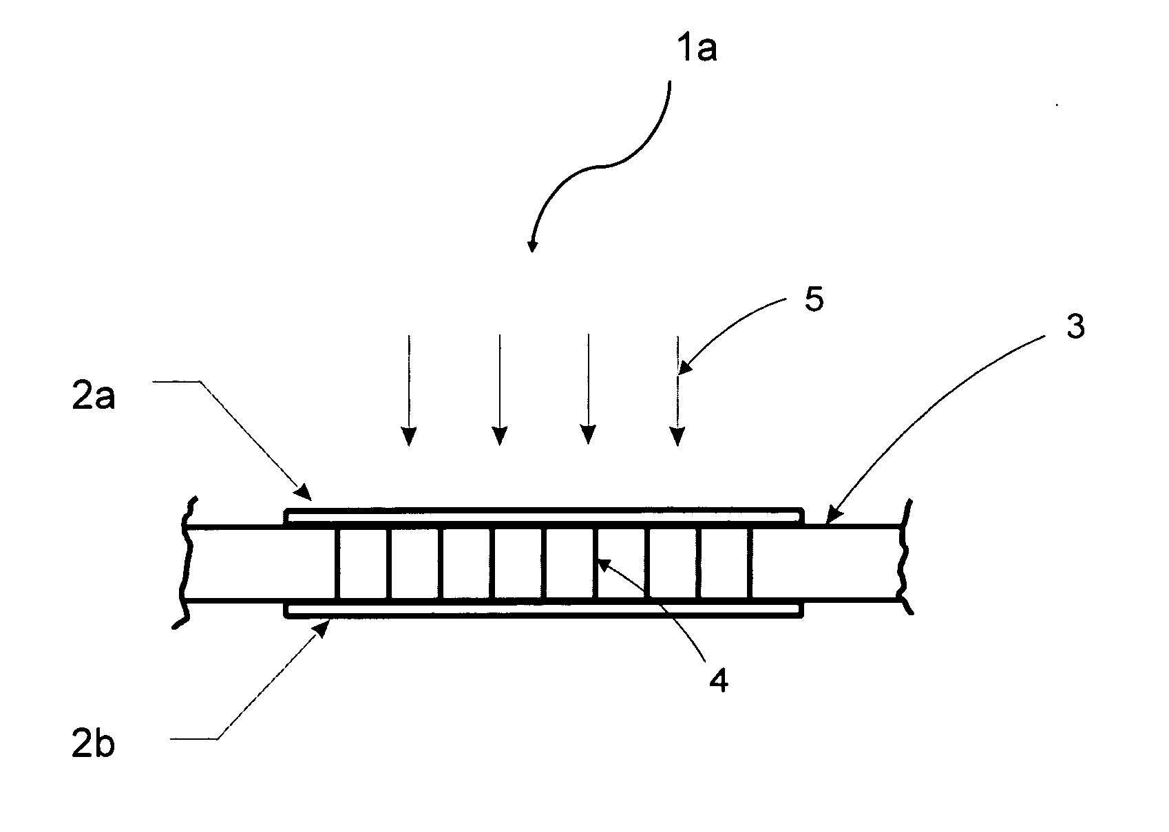
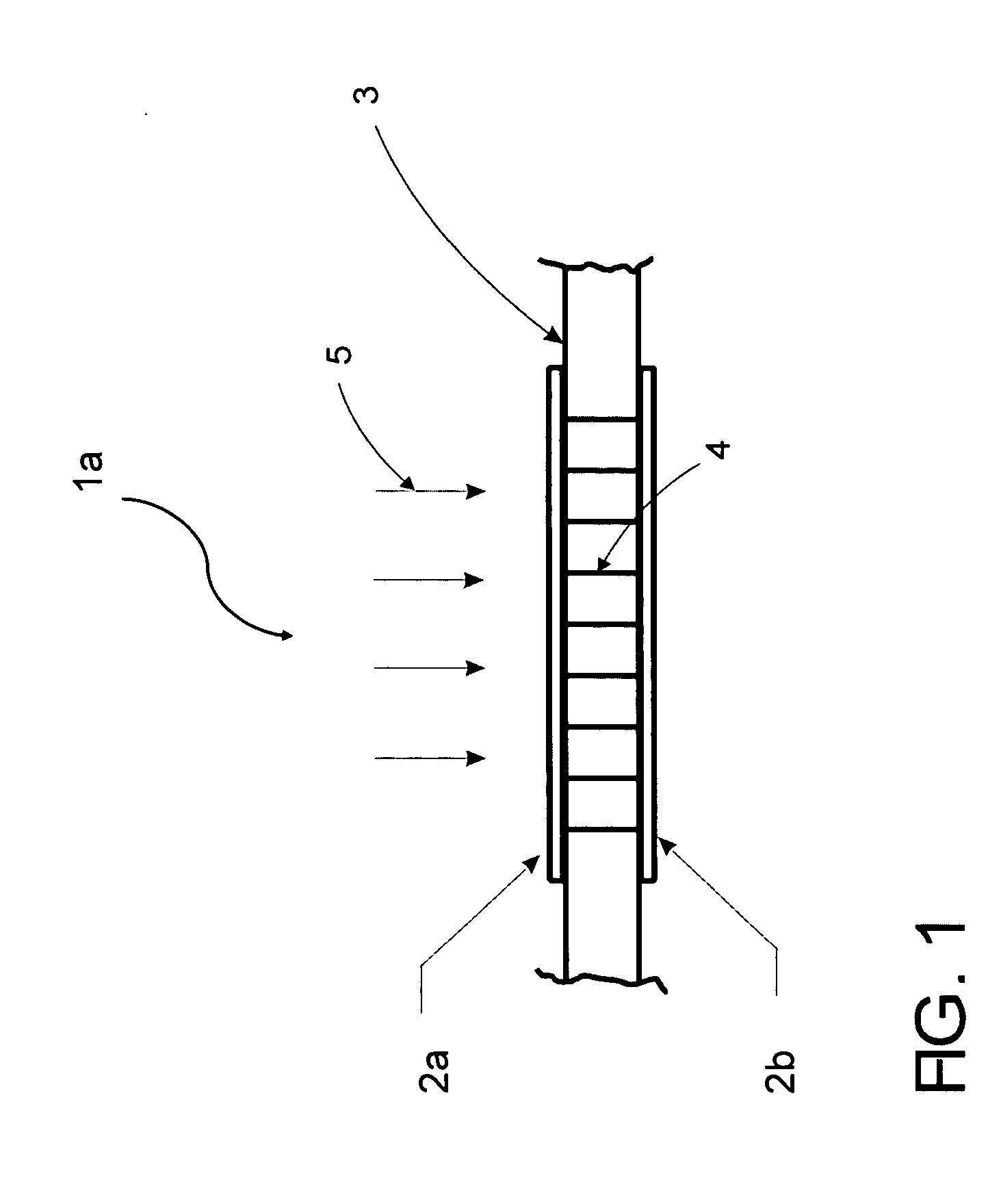
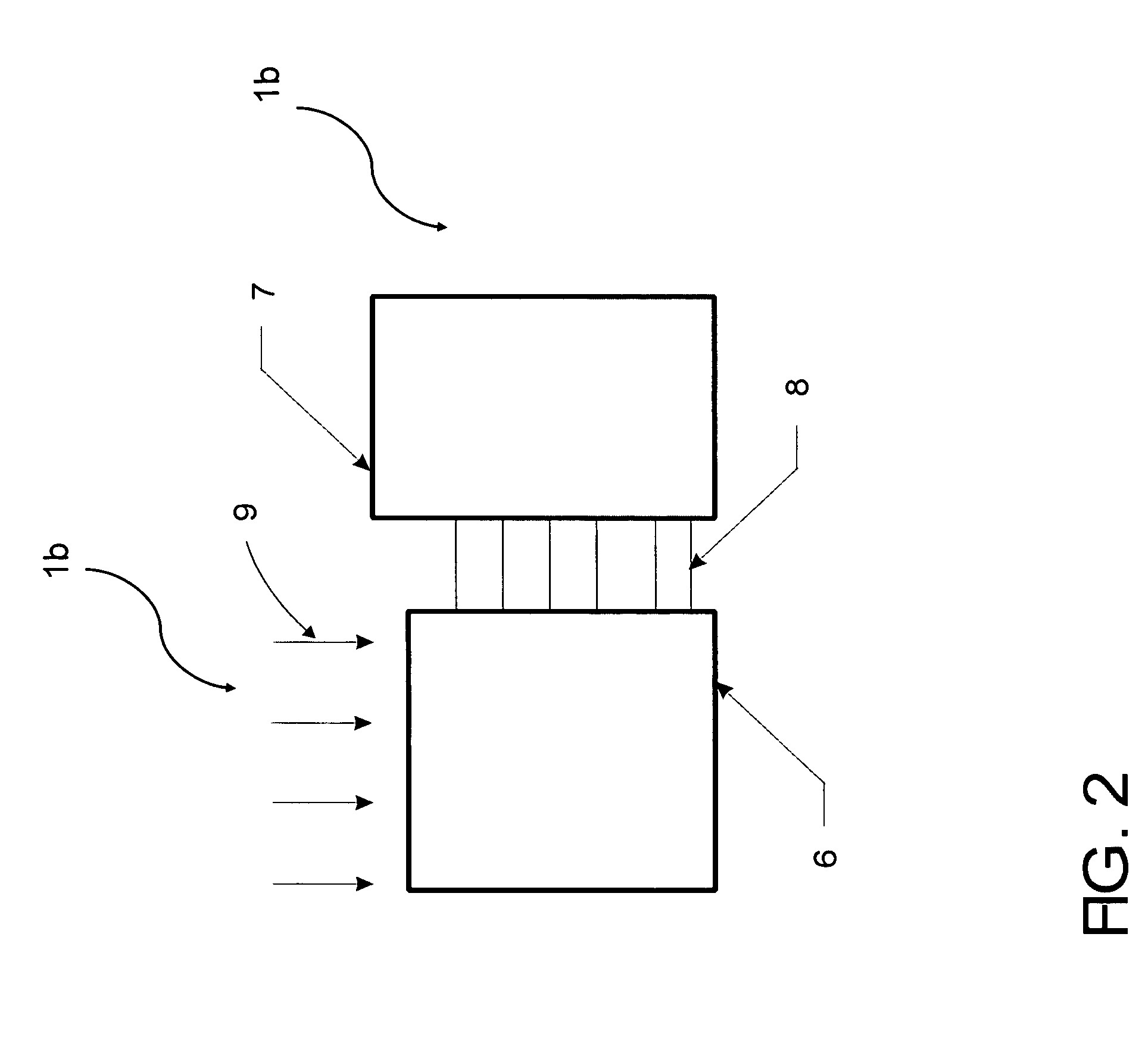
[0027] The following description refers to the accompanying drawings that illustrate certain embodiments of the present invention. Other embodiments are possible and modifications may be made to the embodiments without departing from the spirit and scope of the invention. Therefore, the following detailed description is not meant to limit the present invention. Rather, the scope of the present invention is defined by the appended claims.

[0028] It should be understood that the order of the steps of the methods of the invention is immaterial so long as the invention remains operable. Moreover, two or more steps may be conducted simultaneously unless otherwise specified. In addition, it should be understood that the terms “a,”“an,” and “the” mean “one or more,” unless expressly specified otherwise.

[0029] Prior to describing different aspects and embodiments of the invention in detail, an introduction to some of the characteristic terminology used herein may prove informative. However...


PUM


Abstract

In one aspect, the invention relates to a device for transporting charge carriers. The device includes two conducting regions connected by a nanochannel adapted for transporting a charge carrier. The nanochannel has a cross-sectional dimension less than or equal to the mean free path (MFP) of the charge carrier. Electrical devices including patterned and interconnected conducting layers are described herein whose interconnections are of nanoscale size and whose properties are determined by the shape and size of the interconnections.

Description

CROSS REFERENCE TO RELATED APPLICATIONS [0001] This application claims the benefit of the following U.S. Provisional Applications, namely, U.S. Provisional Application No. 60 / 566,695 filed on May 1, 2004, U.S. Provisional Application No. 60 / 573,164 filed on May 22, 2004, and U.S. Provisional Application No. 60 / 616,654 filed on Oct. 6, 2004. The disclosures of which are herein incorporated by reference in their entirety.FIELD OF THE INVENTION [0002] The invention relates generally to devices and methods for controlling the movement of charge carriers and in particular, devices and methods of altering electrical properties by applying a potential across a nanochannel. BACKGROUND OF THE INVENTION [0003] The number of devices that operate based upon voltage changes and the propagation of electric current is staggering. Only more staggering is the extent that modern day consumers and industrial users depend on such devices. Integrated circuits, communication devices, computers, detectors...

Claims


Application Information

Patent Timeline
Patent Type & Authority Applications(United States)
IPC IPC(8): H01L23/58H01L29/10H01L29/744H01L29/76H01L49/00
CPCB82Y10/00H01L29/7613H01L29/7606H01L29/1025
Inventor JONES, CHRISTOPHER CROFT
Owner JONES CHRISTOPHER CROFT
Why Eureka
Try Eureka