Organic electroluminescent display element, display device having the same, and manufacturing method of the same

a technology of organic electroluminescent display element and manufacturing method, which is applied in the direction of discharge tube luminescnet screen, discharge tube/lamp details, electric discharge lamps, etc., can solve the problems of high manufacturing cost and low light transmittance of low resistance metal materials, and achieve the effect of reducing cost and cos

Active Publication Date: 2005-11-17
SHARP KK
View PDF19 Cites 74 Cited by
  • Summary
  • Abstract
  • Description
  • Claims
  • Application Information

AI Technical Summary

Benefits of technology

[0039] A wet process such as an ink jet method requires a smaller number of steps as compared to a conventional film formation method such as a vapor deposition method, and therefore can be conducted at lower cost. Accordingly, the manufacturing method of the third aspect enables an organic EL display element to be manufactured at lower cost.

Problems solved by technology

However, such a low resistance metal material has a low light transmittance.
A manufacturing process of the organic EL display device 200 thus includes a large number of steps and is complicated, resulting in high manufacturing cost.

Method used


Image

  • Organic electroluminescent display element, display device having the same, and manufacturing method of the same
  • Organic electroluminescent display element, display device having the same, and manufacturing method of the same
  • Organic electroluminescent display element, display device having the same, and manufacturing method of the same

Examples


Embodiment Construction

[0048] Hereinafter, embodiments of the present invention will be described in detail with reference to the accompanying drawings.

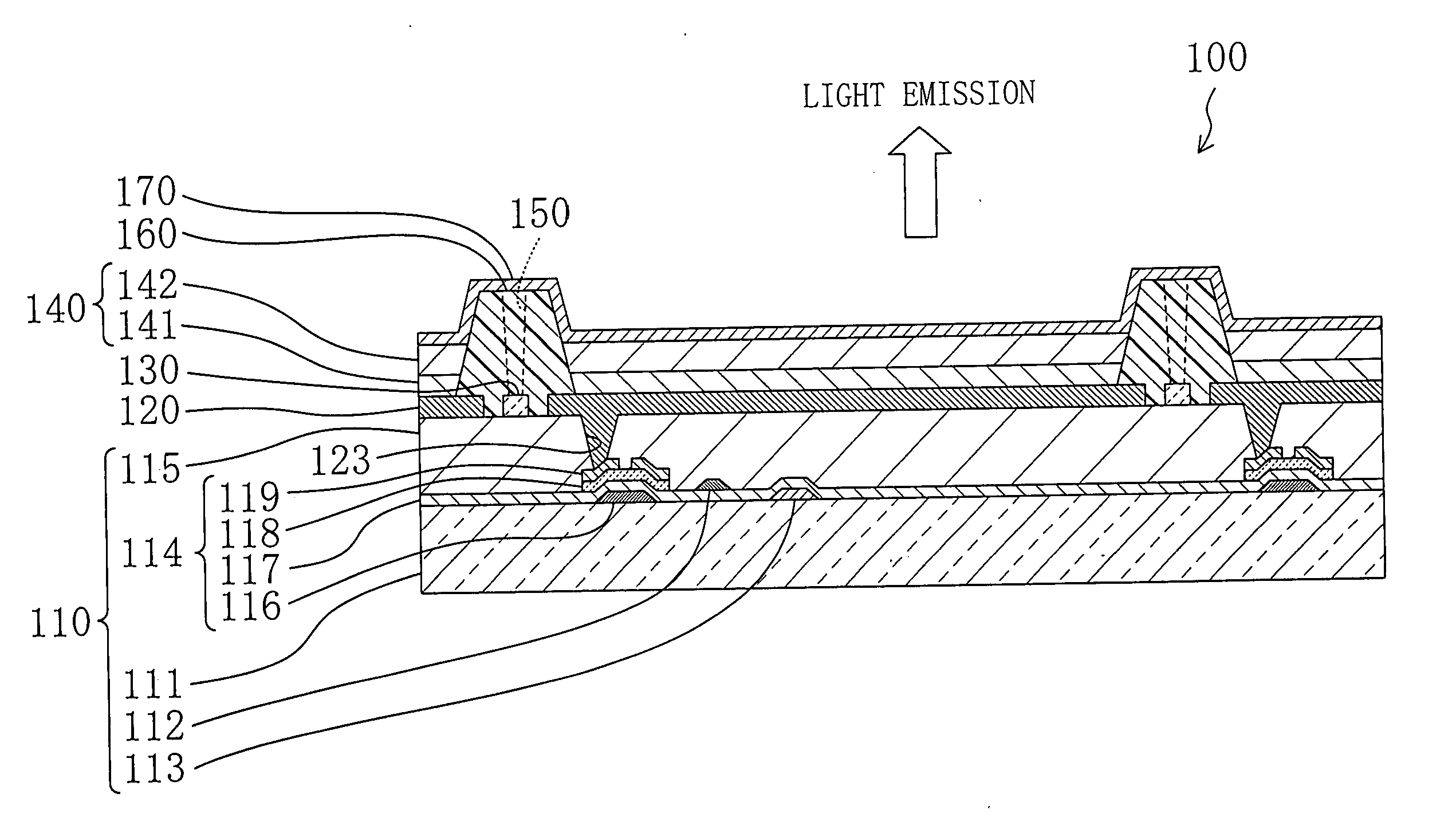
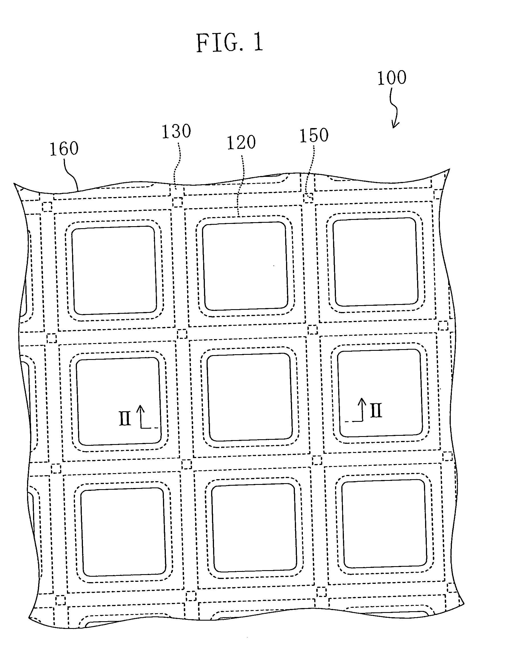
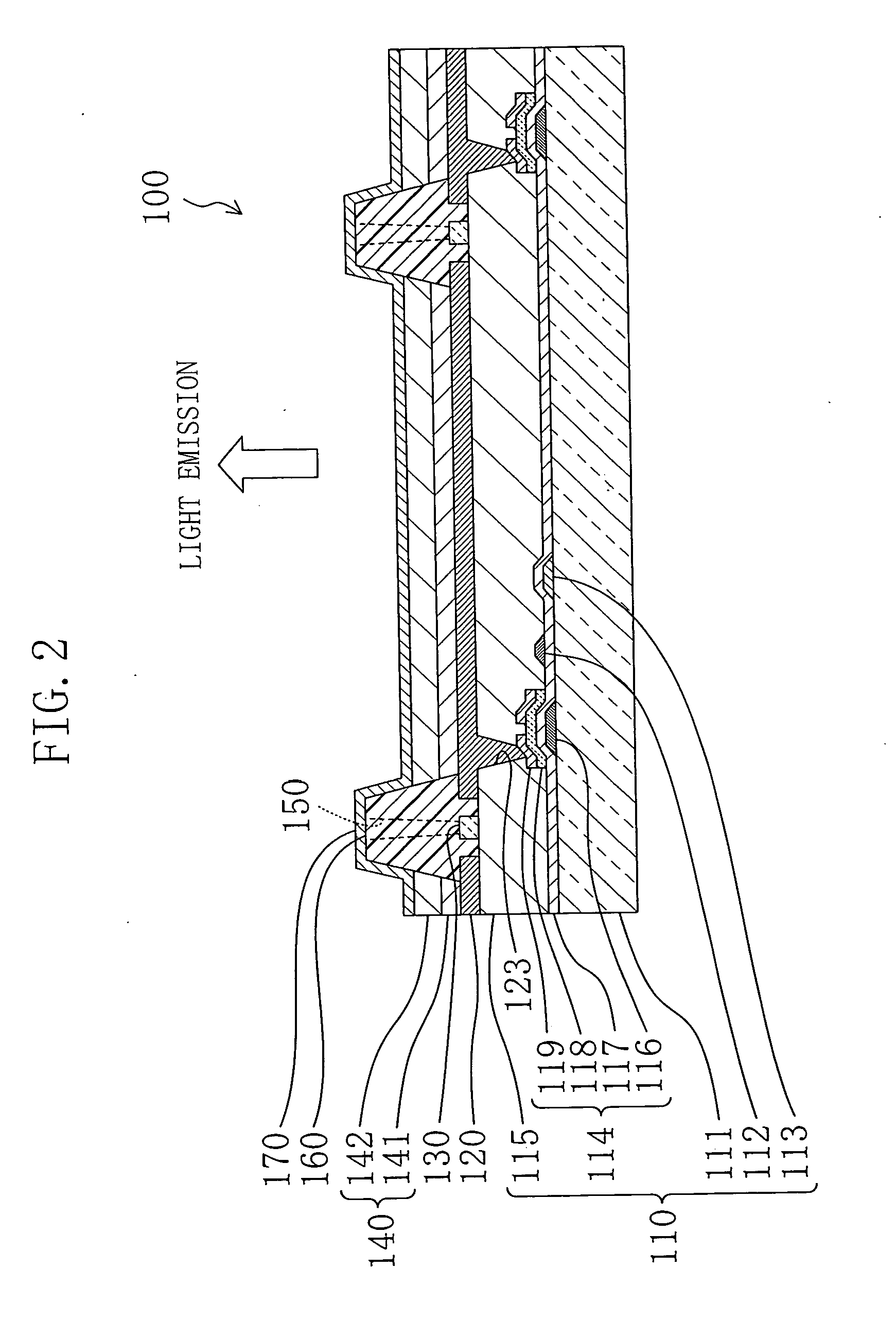
[0049]FIG. 1 is a plan view of an organic EL display element 100 according to an embodiment of the present invention.

[0050]FIG. 2 is a schematic cross-sectional view taken along line II-II of FIG. 1.

[0051] The organic EL display element 100 includes a substrate 110, a plurality of first electrodes 120, an auxiliary electrode 130, an insulating layer 160, a plurality of organic layers 140, and a second electrode 170. The plurality of first electrodes 120 are arranged in a prescribed pattern on the substrate 110. The auxiliary electrode 130 is provided between the first electrodes 120 on the substrate 110 and is separated from the first electrodes 120. The insulating film 160 separates the plurality of first electrodes 120 from each other. The plurality of organic layers 140 are formed on the respective first electrodes 120. The second electrode 170 cover...


PUM


Abstract

An organic electroluminescent display element includes a substrate, a plurality of first electrodes, an auxiliary electrode, an insulating layer, an organic layer, a second electrode, and a conductive material. The auxiliary electrode is provided between the plurality of first electrodes on the substrate and separated from the plurality of first electrodes. The insulating layer covers the auxiliary electrode, separates and isolates the plurality of first electrodes from each other, and has through holes extending to the auxiliary electrode. The organic layer is provided on each of the plurality of first electrodes. The second electrode covers a whole surface of the insulating layer and the organic layers and allowing light emitted in the organic layers to transmit therethrough. The conductive material is provided in the through holes, for electrically connecting the auxiliary electrode to the second electrode.

Description

CROSS REFERENCE TO RELATED APPLICATIONS [0001] This application claims priority under 35 U.S.C. §119 on Patent Application No. 2004-146618 filed in Japan on May 17, 2004, the entire contents of which are hereby incorporated by reference. BACKGROUND OF THE INVENTION [0002] 1. Field of the Invention [0003] The present invention relates to an organic electroluminescent display element, a display device having the organic electroluminescent display element, and a manufacturing method of the organic electroluminescent display element. [0004] 2. Description of the Background Art [0005] Flat panel display elements have less power consumption than that of conventionally used cathode ray tubes (CRTs) and enable reduction in thickness of display elements. Flat panel display elements have therefore been increasingly demanded in response to recent diversification of information processing equipments. Examples of flat panel display elements include liquid crystal display elements and electrolumi...

Claims


Application Information

Patent Timeline
Patent Type & Authority Applications(United States)
IPC IPC(8): H01L27/32H05B33/26H01L51/50H01L51/52H05B33/10H05B33/12H05B33/14H05B33/22H05B33/28
CPCH01L27/3246H01L51/5228H01L2227/323H01L51/5284H01L51/5234H10K59/122H10K50/824H10K50/828H10K50/865H10K59/1201
Inventor OKANO, KIYOSHI
Owner SHARP KK
Why Eureka
Try Eureka