Controlled multi-step magnetron sputtering process

a magnetron sputtering and multi-step technology, applied in the field of plasma sputtering, can solve the problems of high aspect ratio, high aspect ratio, and inability to easily classify barriers, etc., and achieve the effect of improving the conformality of a layer and high-energy ionized target materials

Inactive Publication Date: 2005-11-17
GOPALRAJA PRABURAM +6
View PDF18 Cites 35 Cited by
  • Summary
  • Abstract
  • Description
  • Claims
  • Application Information

AI Technical Summary

Benefits of technology

[0024] In one advantageous aspect of the invention, the target covers both the spindle and the rim of the yoke as well as forming the vault, thereby eliminating any yoke sputtering.
[0025] According to another aspect of the invention, the relative amount of sputtering of the top wall of the inverted vault relative to the sidewalls may be controlled by increasing the magnetic flux in the area of the top wall. An increase of magnetic flux at the sidewalls may result in a predominantly radial distribution of magnetic field between the two sidewalls, resulting in large sputtering of the sidewalls.
[0027] The target may be formed with more than one annular vault on the side facing the substrate. Each vault should have a width of at least 2.5 cm, preferably at least 5 cm, and more preferably at least 7 cm. The width is thus at least 10 times and preferably at least 25 times the dark space, thereby allowing the plasma sheath to conform to the vault outline.
[0031] Instead of using a pre-clean step (for example, a sputter etch clean step), in accordance with one aspect of the present invention, a simultaneous clean-deposition step (i.e., a self-clean deposition step) is carried out. The inventive self clean deposition is carried out using a PVD deposition chamber that is capable of producing high-energy ionized target material. In accordance with one embodiment of the present invention, the high-energy ions physically remove material on flat areas of a wafer. In addition, the high-energy ions can dislodge material from a barrier layer disposed at the bottom of a contact / via feature. Further, in accordance with one embodiment of the present invention, wherein an initial thickness of the barrier layer is small, the high-energy ions can remove enough material from the barrier layer to provide direct contact between a seed layer and the underlying metal (for example, between a copper underlying layer and a copper seed layer). In addition to providing direct contact between the two copper layers, the inventive sputtering process also causes redeposition of copper over sidewalls of the contact / via to reinforce the thickness of the copper seed layer on the sidewall. This provides an improved path for current conduction, and advantageously improves the conformality of a layer subsequently deposited by electroplating.

Problems solved by technology

However, some materials such as barrier materials, for example, TiN, are not so easily classified.
However, sputtering has an inherent disadvantage when a material needs to be filled into a deep narrow hole, that is, one having a high aspect ratio.
The same disadvantage obtains when a thin layer of the material needs to be coated onto the sides of the hole, which is often required for barrier materials.
Contacts to the underlying silicon present a larger problem, but may still be accomplished with either aluminum or copper.
Due to continued downward scaling of the critical dimensions of microcircuits, critical electrical parameters of integrated circuits, such as contact and via resistances, have become more difficult to achieve.
HDP sputter reactors, however, have disadvantages.
They involve a somewhat new technology and are relatively expensive.
Furthermore, the quality of the sputtered films they produce is often not the best, typically having an undulatory surface.
Also, high-energy ions, particularly the argon ions which are also attracted to the wafer, tend to damage the material already deposited.
The small area of the magnetron may require circumferential scanning of the magnetron in a rotary motion at the back of the target to achieve even a minimal level of uniformity, and even with rotary scanning, radial uniformity is difficult to achieve.
High-capacity power supplies are expensive and necessitate complicated target cooling.
The facing pair geometry has the disadvantage that the magnets are stationary and create a horizontally extending field that is inherently non-uniform with respect to the wafer.
This structure has the disadvantage that the soft magnetic material forming the two poles, particularly the central spindle, are exposed to the plasma during sputtering and inevitably contaminate the sputtered layer.
Furthermore, the coil drive provides a substantially cylindrical geometry, which may not be desired in some situations.
Also, the disclosure illustrates a relatively shallow geometry for the target vault, which does not take advantage of some possible beneficial effects for a concavely shaped target.
However, Helmer et al. admit that uniformity of deposition with this magnetic configuration is not good.
Furthermore, the process deleteriously also removes the barrier at the bottom of the trench in a dual-damascene structure.
With shrinking dimension of the integrated circuits, the efficacy of the pre-clean step, as well as sidewall coverage of the seed layer within the contact / via feature, become more problematical.

Method used


Image

  • Controlled multi-step magnetron sputtering process
  • Controlled multi-step magnetron sputtering process
  • Controlled multi-step magnetron sputtering process

Examples


first embodiment

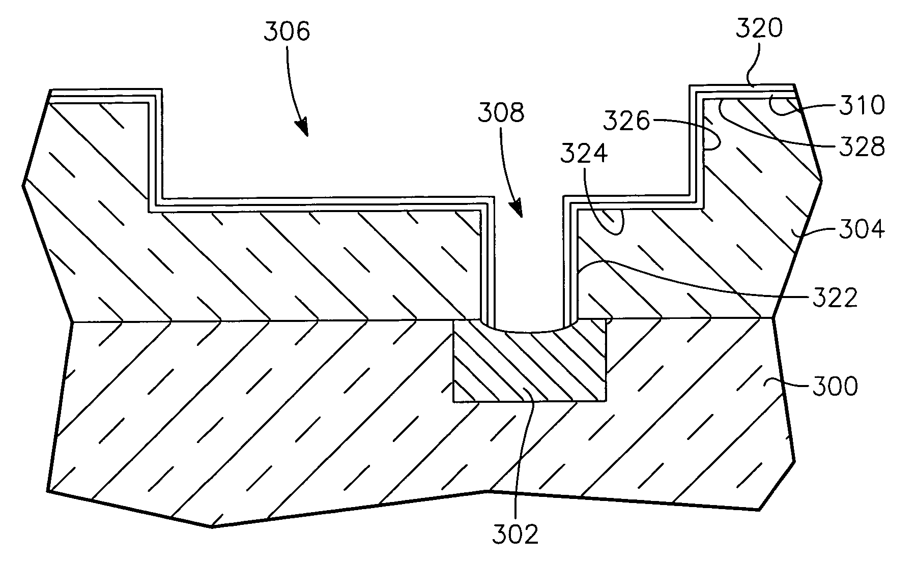
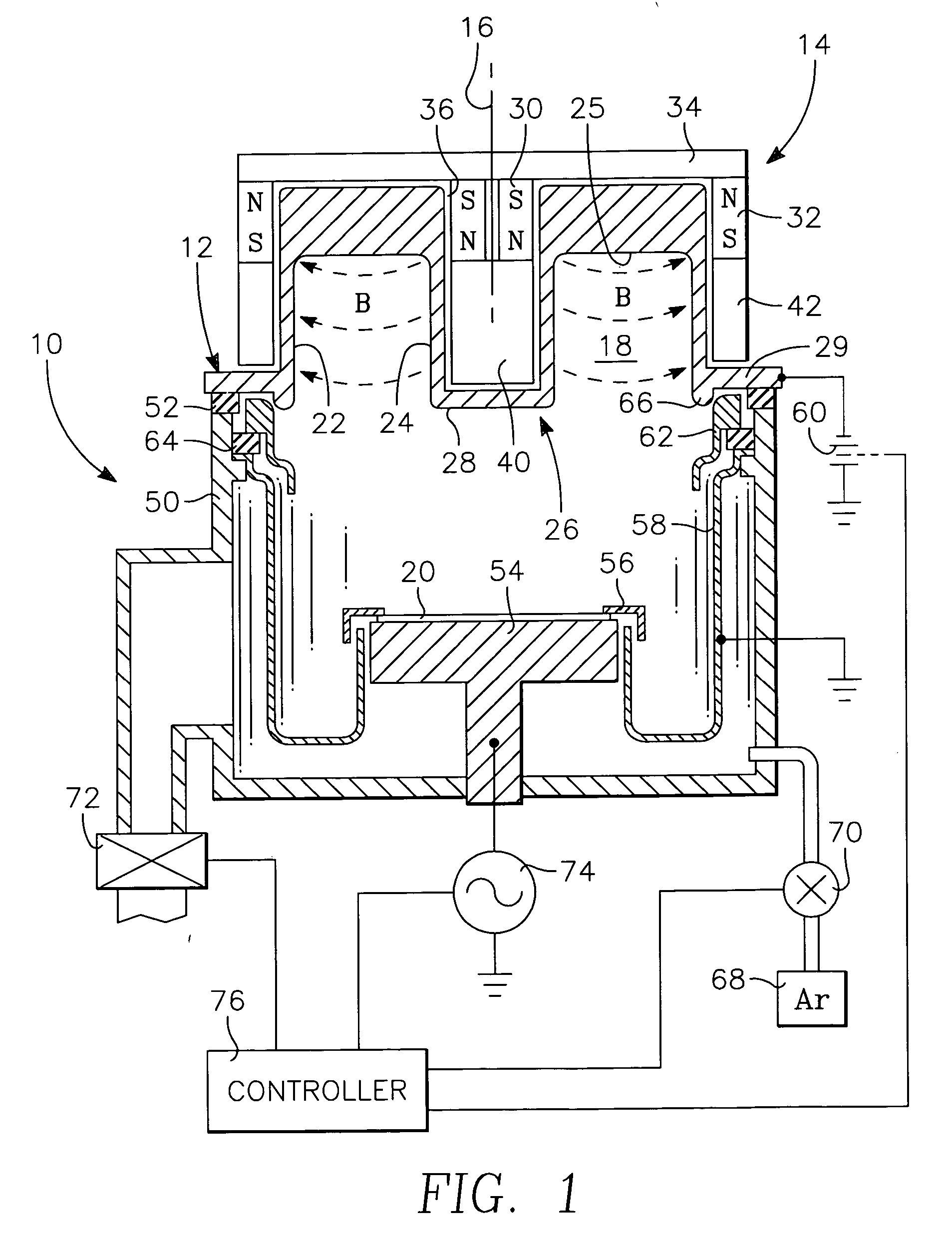
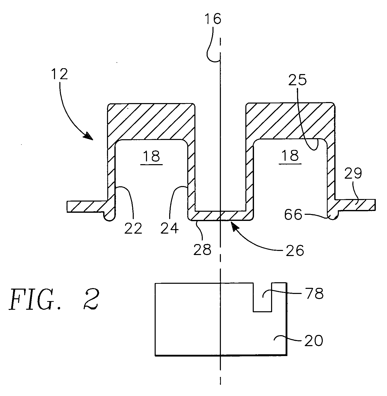
[0053] A magnetron sputter reactor 10 of the invention is illustrated in the schematic cross-sectional view of FIG. 1. It includes a specially shaped sputter target 12 and magnetron 14 symmetrically arranged about a central axis 16 in a reactor otherwise described for the most part by Chiang et al. in the above referenced patent application. This reactor and associated processes will be referred to as SIP+ sputtering in contrast to the SIP sputter reactor of Chiang et al., which uses a planar target. The shaped target 12 or at least its interior surface is composed of the material to be sputter deposited. The invention is particularly useful for sputtering copper, but it may be applied to other sputtering materials as well. It is understood that target may be composed of alloys, typically to less than 10% of alloying. For example, copper is often alloyed with silicon, aluminum, or magnesium. As is known, reactive sputtering of materials like TiN and TaN can be accomplished by using ...

second embodiment

[0064] A sputter reactor 80 of second embodiment of the invention is illustrated in the schematic cross-sectional view of FIG. 3. A magnetron 82 includes the previously described inner magnets 30 and inner pole piece 40. However, one or more outer magnets 84 and an outer pole piece 86 extend around only a segment of the circumference of the target, for example between 15° and 9°. An asymmetric magnetic yoke 88 shaped as a sector magnetically couples the inner and outer magnets 30, 84 but only on the side of target well 36 toward the outer magnets 84. In fact, a circular yoke 88, although larger, would not affect the operative magnetic field. As a result, a high-density plasma is generated in only a small circumferential portion of the target vault 18. For self-ionized plating (SIP) and particularly sustained self-sputtering (SSS), a high plasma density is desired. In view of the limited capacity of realistic power supplies 60, the high plasma density can be achieved by reducing the ...

third embodiment

[0066] Other magnet configurations are possible to produce similar magnetic field distributions. A sputter reactor 100 of the invention is illustrated in the schematic cross-sectional view of FIG. 4 A magnetron 102 includes an inner magnet 104 having a magnetization direction generally aligned with a radius of the target 12 about the target axis 16. One or more outer magnets 106 are similarly radially magnetized but anti-parallel to the magnetization of the inner magnet 104 with respect to the center of the vault 18. A C-shaped magnetic yoke has two arms 110, 112 in back of and supporting the respective magnets 104, 106 and a connector 114 supported on and rotated by the shaft of the motor 90.

[0067] The magnets 104, 106 may be advantageously positioned only on reduced circumferential portions of the sidewalls 24, 22 of the target vault 18 so as to concentrate the magnetic field there. Furthermore, in this configuration extending along only a small segment of the target periphery, th...


PUM

PropertyMeasurementUnit
widthaaaaaaaaaa
widthaaaaaaaaaa
widthaaaaaaaaaa

Abstract

A multi-step sputtering process in plasma sputter reactor having target and magnetron operable in two modes, for example, in a substrate sputter etch and a substrate sputter deposition. The target has an annular vault facing the wafer to be sputter coated. Various types of magnetic means positioned around the vault create a magnetic field supporting a plasma extending over a large volume of the vault. An integrated copper via filling process with the inventive reactor or other reactor includes a first step of highly ionized sputter deposition of copper, which can optionally be used to remove the barrier layer at the bottom of the via, a second step of more neutral, lower-energy sputter deposition of copper to complete the seed layer, and a third step of electroplating copper into the hole to complete the metallization. The first two steps can be also used with barrier metals.

Description

RELATED APPLICATIONS [0001] This application is a division of Ser. No. 10 / 934,231, filed Sep. 3, 2004, which is a division of Ser. No. 10 / 197,680, filed Jul. 16, 2002, now issued as U.S. Pat. No. 6,787,006, which is a division of Ser. No. 09 / 703,601, filed Nov. 1, 2000, now issued as U.S. Pat. No. 6,451,177, which is a continuation in part of Ser. No. 09 / 518,180, filed Mar. 2, 2000, now issued as U.S. Pat. No. 6,277,249, which is a continuation in part of Ser. No. 09 / 490,026, filed Jan. 21, 2000, now issued as U.S. Pat. No. 6,251,242. The application is also related to Ser. No. 09 / 703,738, filed Nov. 1, 2000, now issued as U.S. Pat. No. 6,406,599.FIELD OF THE INVENTION [0002] The invention relates generally to plasma sputtering. In particular, the invention relates to the sputter target and associated magnetron used in a sputter reactor and to an integrated via filling process using sputtering. BACKGROUND ART [0003] A semiconductor integrated circuit contains many layers of differen...

Claims


Application Information

Patent Timeline
Patent Type & Authority Applications(United States)
IPC IPC(8): C23C14/04C23C14/34C23C14/16C23C14/32C23C14/35H01J37/34H01L21/203H01L21/285H01L21/288H01L21/768
CPCC23C14/046H01L2221/1089C23C14/185C23C14/225C23C14/35H01J37/3405H01J37/342H01J37/3423H01J37/3452H01J37/3455H01J37/3458H01L21/2855H01L21/76805H01L21/76843H01L21/76844H01L21/76862H01L21/76865H01L21/76873C23C14/165C23C14/352
Inventor GOPALRAJA, PRABURAMFU, JIANMINGCHEN, FUSENDIXIT, GIRISHXU, ZHENGWANG, WEISINHA, ASHOK K.
Owner GOPALRAJA PRABURAM
Why Eureka
Try Eureka