Method of cvd for forming silicon nitride film on substrate

a silicon nitride film and substrate technology, applied in the direction of coatings, chemical vapor deposition coatings, metallic material coating processes, etc., can solve the problem of bringing about the controllability of the film thickness in the cleaning process subsequently performed, and achieve the controllability of the film thickness of the silicon nitride film at the low process temperature of film-formation

Inactive Publication Date: 2005-11-17
TOKYO ELECTRON LTD
View PDF2 Cites 110 Cited by
  • Summary
  • Abstract
  • Description
  • Claims
  • Application Information

AI Technical Summary

Benefits of technology

[0006] An object of the present invention is to provide a CVD method for forming a silicon nitride film on a target substrate, which can employ a relatively low process temperature of film-formation, while allowing a cleaning process to be subsequently performed with high controllability in the film thickness of the silicon nitride film.

Problems solved by technology

As described later, however, the present inventors have found that an insulating film formed by conventional film-formation methods of this kind causes a problem in a cleaning process subsequently performed.
Specifically, where a lower process temperature of film-formation is used in conventional film-formation methods, the etching rate of an insulating film becomes higher, thereby bringing about lower controllability in the film thickness in the cleaning process subsequently performed.

Method used


Image

  • Method of cvd for forming silicon nitride film on substrate
  • Method of cvd for forming silicon nitride film on substrate
  • Method of cvd for forming silicon nitride film on substrate

Examples


first embodiment

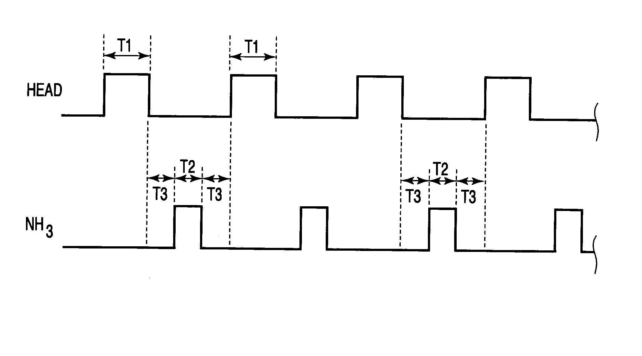
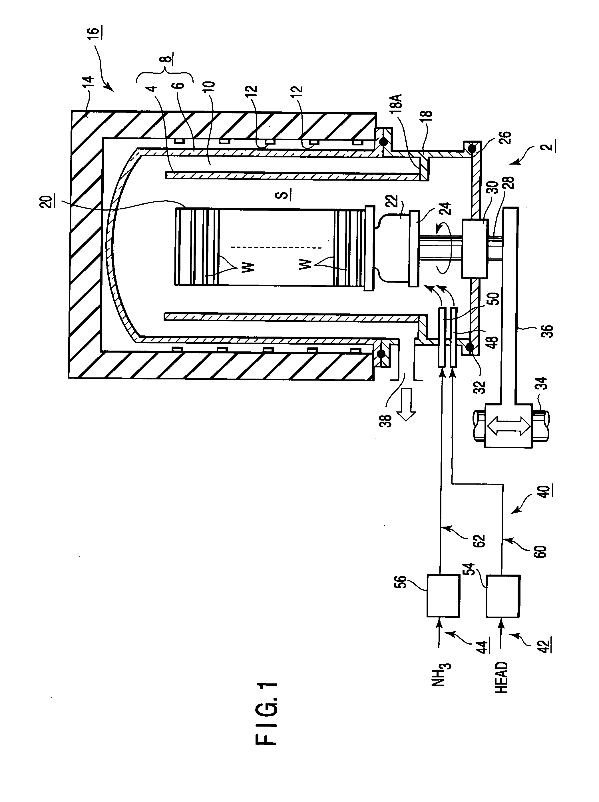
[0025]FIG. 1 is a sectional view showing a film-formation apparatus (vertical CVD apparatus) according to a first embodiment of the present invention. The film-formation apparatus 2 is arranged to supply a process gas including hexaethylaminodisilane [C12H36N6Si2] (which will be referred to as HEAD, as well) gas used as a silicon-containing material gas, and NH3 gas, so as to deposit a silicon nitride film (which will be referred to as SiN, as well).

[0026] The film-formation apparatus 2 includes a process container 8 having a double tube structure, which is formed of an inner tube 4 and an outer tube 6. The inner tube 4 and outer tube 6 are formed of cylindrical quartz bodies, and disposed concentrically with each other with a predetermined gap 10 therebetween. The process container 8 is surrounded by a heating cover 16, which includes a heater 12, such as an electrical heater, and a thermal insulator 14. The heater 12 is disposed over the entire inner surface of the thermal insula...

second embodiment

[0050]FIG. 3 is a sectional view showing a film-formation apparatus (vertical CVD apparatus) according to a second embodiment of the present invention. FIG. 4 is a sectional plan view showing part of the apparatus shown in FIG. 3. The film-formation apparatus 130 is arranged to alternately supply a first process gas including hexaethylaminodisilane (HEAD) gas, and a second process gas including NH3 gas, so as to deposit a silicon nitride film.

[0051] The apparatus 130 is of a plasma-processing type and includes a process container 132 shaped as a cylindrical column with a ceiling and an opened bottom. The entirety of the process container 132 is made of, e.g., quartz. The top of the process container 132 is provided with a quartz ceiling plate 134 to airtightly seal the top. The bottom of the process container 132 is connected through a seal member 138, such as O-ring, to a cylindrical manifold 136.

[0052] The cylindrical manifold 136 is made of, e.g., stainless steel, and supports ...


PUM

PropertyMeasurementUnit
temperatureaaaaaaaaaa
pressureaaaaaaaaaa
thicknessaaaaaaaaaa

Abstract

A CVD method is to form a silicon nitride film on a target substrate (W). The method includes heating the substrate (W) accommodated in a process container (8), at a process temperature, and supplying a process gas including hexaethylamino-disilane gas and ammonia gas onto the substrate (W) heated at the process temperature, thereby depositing a silicon nitride film on the substrate (W).

Description

TECHNICAL FIELD [0001] The present invention relates to a CVD method for forming a silicon nitride film on a target substrate, used in a semiconductor process. The term “semiconductor process” used herein includes various kinds of processes which are performed to manufacture a semiconductor device or a structure having wiring layers, electrodes, and the like to be connected to a semiconductor device, on a target substrate, such as a semiconductor wafer or a glass substrate used for an LCD (Liquid Crystal Display) or FPD (Flat Panel Display), by forming semiconductor layers, insulating layers, and conductive layers in predetermined patterns on the target substrate. BACKGROUND ART [0002] Semiconductor devices include insulating films made of a material, such as SiO2, PSG (Phospho Silicate Glass), P(plasma)-SiO, P(plasma)-SiN, SOG (Spin On Glass), Si3N4 (silicon nitride), etc. [0003] For example, Jpn. Pat. Appln. KOKAI Publication No. 11-172439 discloses a method of forming a silicon o...

Claims


Application Information

Patent Timeline
Patent Type & Authority Applications(United States)
IPC IPC(8): C23C16/34C23C16/46H01L21/318
CPCC23C16/345H01L21/3185C23C16/46C23C16/45542H01L21/02274H01L21/02301H01L21/02219H01L21/02307H01L21/02271H01L21/0217H01L21/324
Inventor KATO, HITOSHIORITO, KOICHIKIKUCHI, HIROYUKIMAKU, SHINGO
Owner TOKYO ELECTRON LTD
Why Eureka
Try Eureka