Light emitting diode apparatuses with heat pipes for thermal management

a technology of light-emitting diodes and heat pipes, which is applied in lighting and heating apparatuses, semiconductor devices for light sources, and semiconductor/solid-state device details. it can solve the problems of resistive elements, high resistive losses in cladding layers, electrodes, printed circuit traces,

Inactive Publication Date: 2005-11-24
GELCORE LLC (US)
View PDF5 Cites 49 Cited by
  • Summary
  • Abstract
  • Description
  • Claims
  • Application Information

AI Technical Summary

Benefits of technology

[0010] According to one aspect, a light emitting apparatus includes one or more light emitting diode chips and a passive heat pipe. The passive heat pipe includes: (i) a generally planar chip support wall on which the one or more light emitting diode chips are disposed; (ii) at least one additional wall sealed with the chip support wall to define a closed interior volume; (iii) a heat transfer fluid disposed in the closed interior volume; and (iv) one or more wicking structures disposed at least on an interior surface of the chip support wall.

Problems solved by technology

A high operating current, in turn, leads to high resistive losses in cladding layers, electrodes, wire bonds, printed circuit traces, or other electrically resistive elements in the current path of the light emitting diode package.
These resistive losses translate into substantial heating of the light emitting diode package when operated at high power levels.
Heating can produce thermal degradation of the light emitting diode chip, the chip electrodes, sealing encapsulant, solder bumps, or other components of the light emitting diode package.
Moreover, heating generally increases the resistance of the electrical pathways and can reduce the light emitting diode operating efficiency.
These design techniques reduce, but do not eliminate, thermal concerns in high brightness light emitting diode packages.
The arrangement of Board et al. is not well suited for distributing heat across an array of light emitting diode devices.
In such an array, thermal management issues include not only removal of heat from the array, but also providing substantially uniform distribution of heat across the array.
The use of the Peltier thermoelectric device for thermal coupling of the light emitting diode device with the heat sink is also problematic, since it increases the complexity of the light emitting apparatus.
These hot spots can be problematic if some chips are disposed over a leg of the serpentine heat pipe, while other chips are disposed between the legs.
Actively driven liquid flow also requires a fluid source and drain, or a closed-loop continuous liquid pumping system, which is unsuitable for many light emitting diode apparatuses and lighting applications.

Method used


Image

  • Light emitting diode apparatuses with heat pipes for thermal management
  • Light emitting diode apparatuses with heat pipes for thermal management
  • Light emitting diode apparatuses with heat pipes for thermal management

Examples


Embodiment Construction

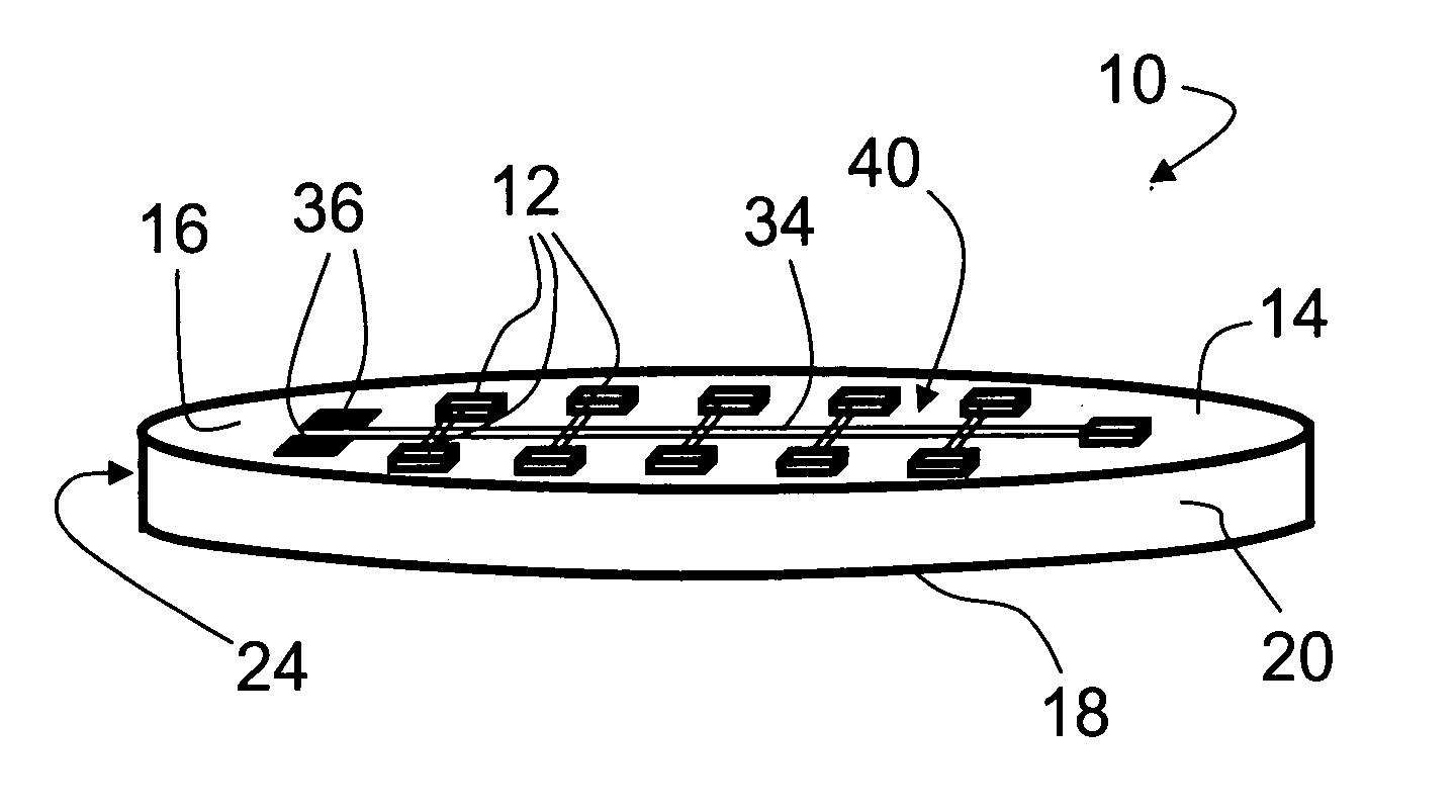
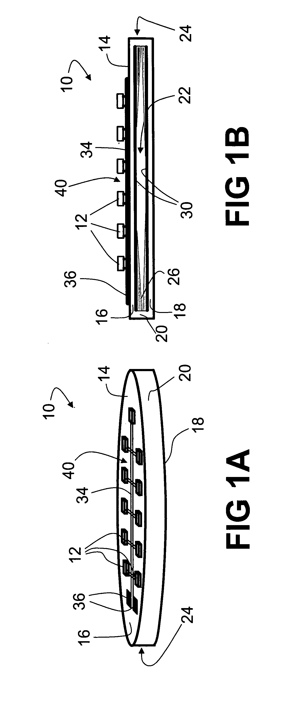
[0022] With reference to FIG. 1, a light emitting package 10 includes a plurality of light emitting diode devices 12 disposed on a generally planar support 14 having a generally circular lateral area. The support 14 includes a first principal wall 16 on which the light emitting diode devices 12 are disposed, a second principal wall 18 opposite the first principal wall 16, and an annular sidewall 20 connecting the first and second principal walls 16, 18 to define a sealed interior volume 22 of a generally planar heat pipe 24. The sealed interior volume 22 is substantially defined by a gap between the first and second principal walls 16, 18. The principal walls 16, 18 preferably have lateral areas larger than the gap between the principal walls 16, 18, so that the support 14 is generally planar with a lateral area larger than its thickness.

[0023] A heat transfer fluid 26 such as water, methanol, or the like, is disposed in the interior volume 22. In FIG. 1 as well as in the other dra...


PUM

PropertyMeasurementUnit
operating voltageaaaaaaaaaa
temperatureaaaaaaaaaa

Abstract

A light emitting apparatus (10, 110, 210, 310, 410) includes one or more light emitting diode chips (12, 112, 212, 312, 412) disposed on a chip support wall (16, 116, 216) including printed circuitry (34, 134, 234, 360, 362, 460, 462) connecting with the light emitting diode chips. A heat pipe (24, 124, 224, 324, 424) has a sealed volume (22, 122, 222, 322, 422) defined by walls including the chip support wall and at least one additional wall (18, 20, 118, 120, 218). The heat pipe further includes a heat transfer fluid (26, 226, 326, 426) disposed in the sealed volume.

Description

BACKGROUND [0001] The present invention relates to the lighting arts. It especially relates to high intensity light emitting diode packages, components, apparatuses, and so forth, and will be described with particular reference thereto. However, the invention will also find application in conjunction with other solid state light emitters such as vertical cavity surface emitting lasers. [0002] High power light emitting diode packages employ one or more light emitting diode devices operating at relatively high current levels to produce high brightness or high light output intensities. A light emitting diode chip has a voltage drop which typically is determined largely by the band gap of the material. The operating voltage of a light emitting diode chip is typically about 4 volts or less. Thus, generating high light output intensities involves increasing the operating current. A high operating current, in turn, leads to high resistive losses in cladding layers, electrodes, wire bonds, ...

Claims


Application Information

Patent Timeline
Patent Type & Authority Applications(United States)
IPC IPC(8): F21K99/00H01L21/00H01L25/075H01L33/64
CPCF21K9/00H01L25/0753H01L33/648H01L2224/16H01L2224/48091F21V29/51H01L2924/00014
Inventor ARIK, MEHMETWEAVER, STANTONBECKER, CHARLES
Owner GELCORE LLC (US)
Why Eureka
Try Eureka