Switched capacitance circuit and analog/digital converter including said circuit

a technology of capacitance circuit and circuit, applied in the direction of transmission system, time-varying network, information storage, etc., can solve the problems of predetermined and unchangeable values of these capacitances, inability to act on the capacitance, and significant increase in power consumption of the comparator cmp

Inactive Publication Date: 2005-11-24
ST ERICSSON SA
View PDF4 Cites 19 Cited by
  • Summary
  • Abstract
  • Description
  • Claims
  • Application Information

AI Technical Summary

Benefits of technology

[0022] The disclosed embodiments of the present invention provide a circuit that obviates the drawbacks and problems of the known technique described above and, more particularly, realize a switched capacitance circuit in which the best performances in terms of input signal sampling speed do not impose an excessive increase of the power consumption or a significant increment of the area occupied by the circuit or both.

Problems solved by technology

When the duration of this transient has to be reduced, it is typically not possible to act on the capacitances of the switched capacitance section because, as is well known to persons skilled in the art, the values of these capacitances are predetermined and unchangeable, since they are essentially imposed by the resolution of the converter.
It has been observed that this solution is associated with some drawbacks.
In particular, the power consumption of the comparator CMP becomes significantly greater when this current is increased.
Though here described with particular reference to an analog / digital converter, these problems are nevertheless quite generally associated with circuits that provide switched capacitances upstream of a converter stage or, more generally, an operational stage.

Method used


Image

  • Switched capacitance circuit and analog/digital converter including said circuit
  • Switched capacitance circuit and analog/digital converter including said circuit
  • Switched capacitance circuit and analog/digital converter including said circuit

Examples


Embodiment Construction

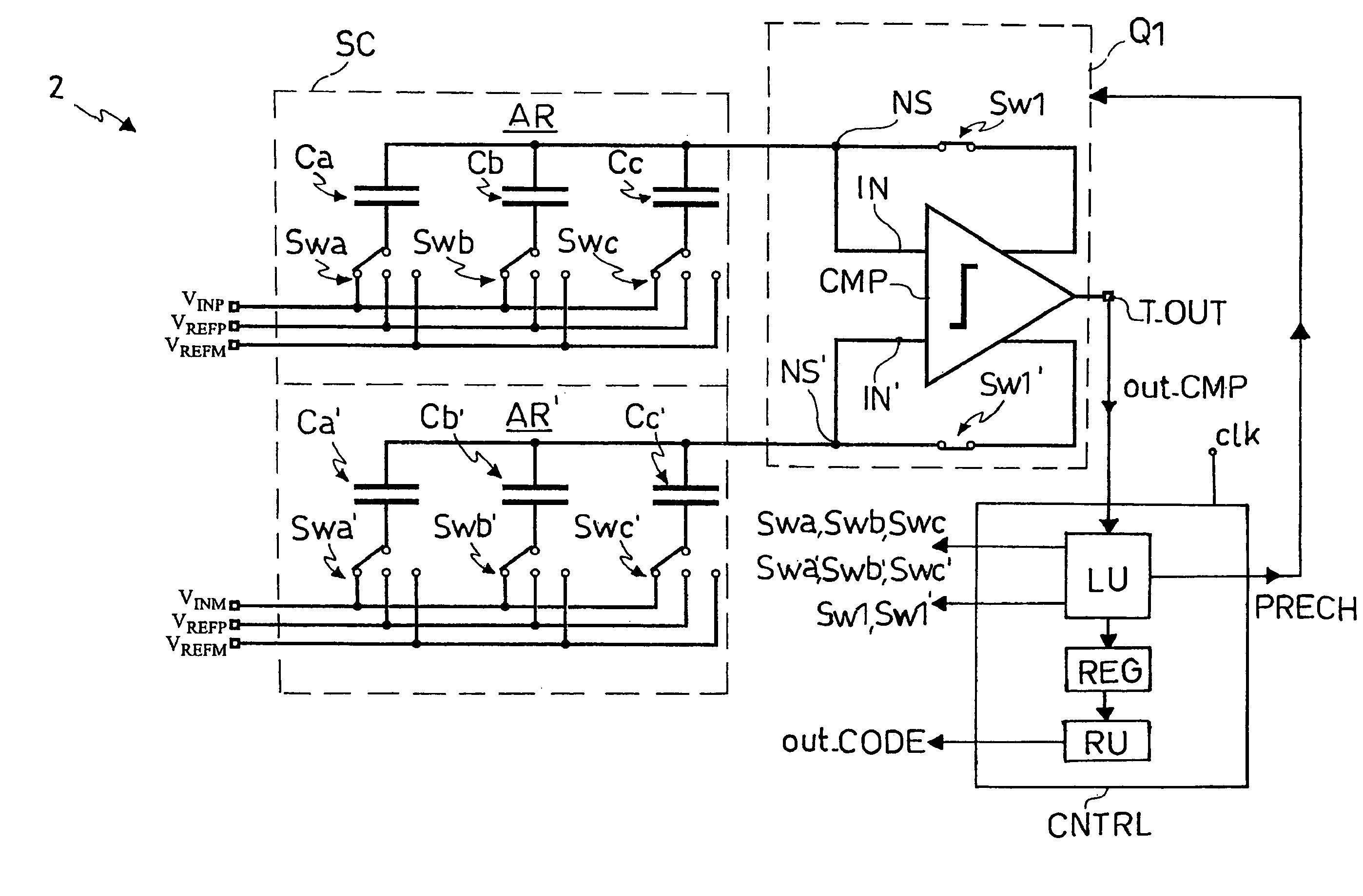
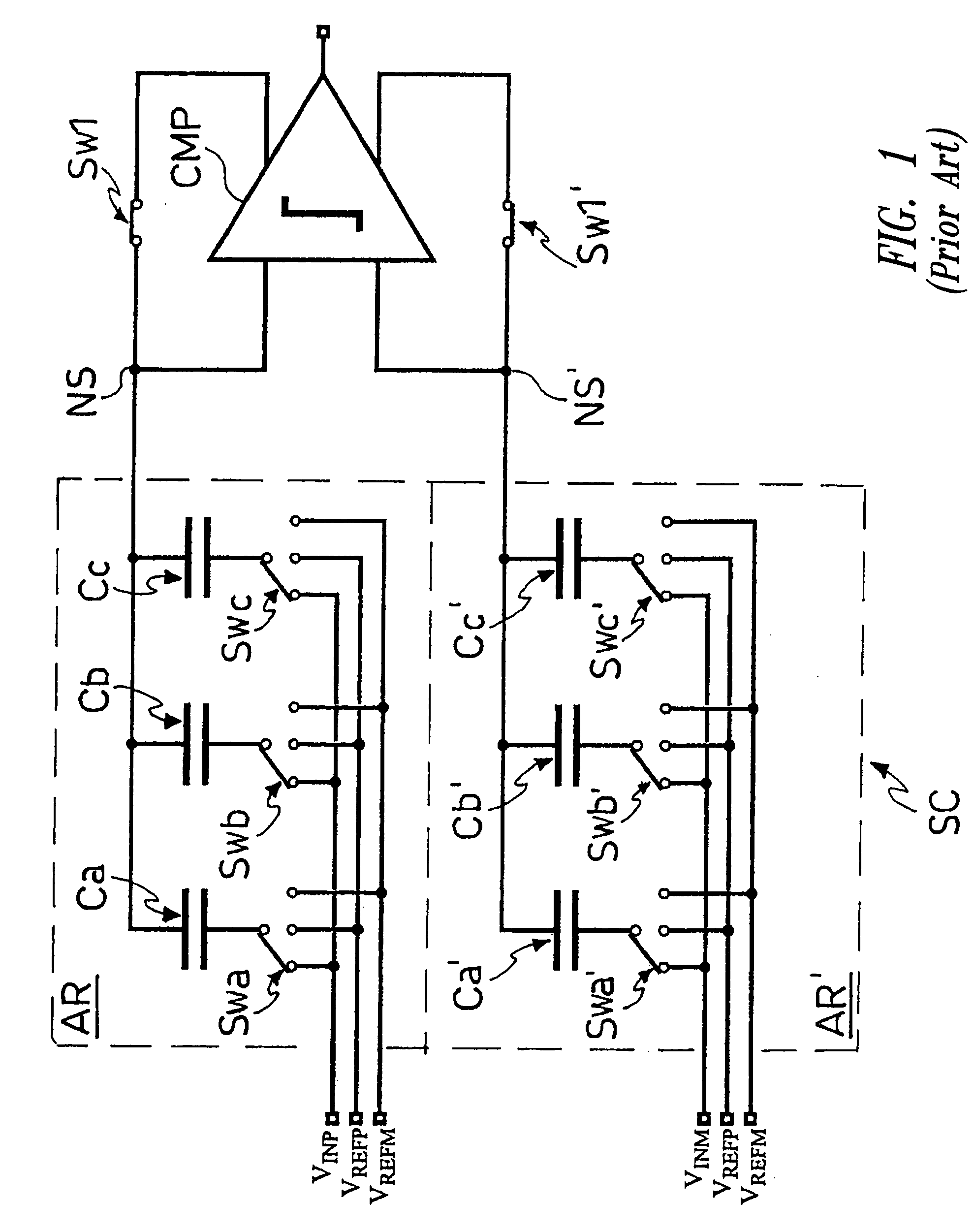
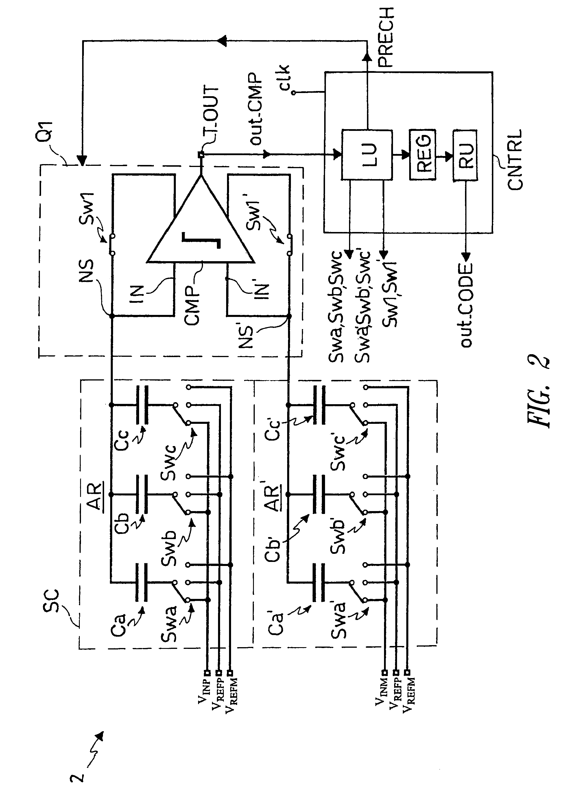
[0033]FIG. 2 shows a simplified schematic circuit layout of a particularly preferred embodiment of a switched capacitance circuit 2 in accordance with the present invention. The switched capacitance circuit 2 includes a switched capacitance section SC, an operational stage CMP, and a control section CNTRL. In this example the operational stage CMP is a voltage comparator comprising a non-inverting input IN, an inverting input terminal IN′ and an output terminal T_OUT.

[0034] In the embodiment of FIG. 2, the switched capacitance circuit 2 is a three-bit analog / digital converter capable of converting an analog differential input signal VINP, VINM into a series of three-bit digital samples out_CODE of that signal. The teachings of the present invention may however be extended without difficulty to analog / digital converters having a greater resolution, for example, ten-bit converters.

[0035] Preferably, the analog / digital converter will be a converter of the SAR type and of the “fully d...


PUM


Abstract

A switched capacitance circuit including: a switched capacitance section, capable of receiving as input a signal and carrying out a sampling of said signal, the section comprising at least one group of capacitors each of which has a terminal connected to a common node; at least an operational stage including at least an input terminal connected to said common node, the operational stage providing a current to said common node for charging said group of capacitors during a sampling time interval of said signal. The circuit further includes an auxiliary circuit connected to said common node and capable of being activated / deactivated by an enabling signal for injecting a further current into said common node and increasing the current provided to said common node during at least one time interval equal to a fraction of said sampling interval.

Description

BACKGROUND OF THE INVENTION [0001] 1. Field of the Invention [0002] The present invention relates to switched capacitance circuits and, more particularly to a switched capacitance circuit having an analog / digital converter circuit. [0003] 2. Description of the Related Art [0004] As is well known, switched capacitance circuits utilize switches, typically MOS (Metal Oxide Semiconductor) transistors, capacitors and operational amplifiers to perform some analog functions that are normally realized by means of resistances, capacitors and operational amplifiers. [0005] Switched capacitance circuit techniques, developed principally for the purpose of rendering possible the simultaneous integration of analog and digital functions in the same integrated circuit, found their most extensive application in the realization of filters and in the realization of circuits for sampling signals and / or converting data. [0006] In particular, applications relating to signal sampling and data conversion m...

Claims


Application Information

Patent Timeline
Patent Type & Authority Applications(United States)
IPC IPC(8): G11C27/02H03H19/00H03K5/24H03M1/00H03M1/06H03M1/12H03M1/46
CPCG11C27/024G11C27/026H03H19/004H03M1/468H03K5/249H03M1/0682H03K5/2481
Inventor CONFALONIERI, PIERANGELOZAMPROGNO, MARCO
Owner ST ERICSSON SA
Why Eureka
Try Eureka