Pixel circuit and display device

a technology of pixel circuit and display device, which is applied in the direction of semiconductor devices, instruments, electrical devices, etc., can solve the problem of not being able to make the lines too wid

Inactive Publication Date: 2005-12-01
SONY CORP
View PDF10 Cites 67 Cited by
  • Summary
  • Abstract
  • Description
  • Claims
  • Application Information

AI Technical Summary

Benefits of technology

[0049] It is desirable to provide a display device able to prevent crosstalk between pixels by relatively simple layout, able to prevent the occurrence of uneven luminance in the displayed image, able to stably and correctly supply a current of a desired value to the light emitting element of each pixel without regard to the variation of the threshold value of the active elements inside the pixels, and as a result able to display a high quality image.
[0050] It is further desirable to provide a pixel circuit and a display device able to stably and correctly supply a current of a desired value to the light emitting element of each pixel without regard to the variation of the threshold value of the active elements inside the pixels and able to stably hold the reference potential even when an offset cancellation function by the precharge potential line is provided and as a result able to display a high quality image.

Problems solved by technology

It is not possible to make the lines too wide due to the constraints in the circuit area.

Method used


Image

  • Pixel circuit and display device
  • Pixel circuit and display device
  • Pixel circuit and display device

Examples


first embodiment

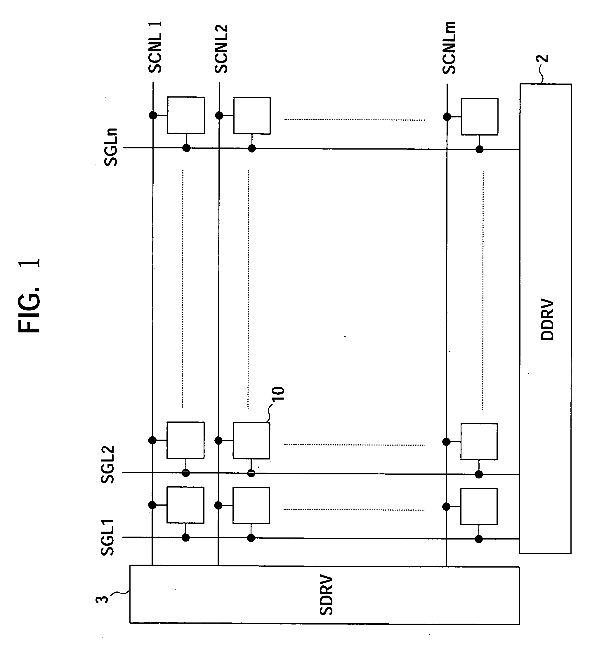
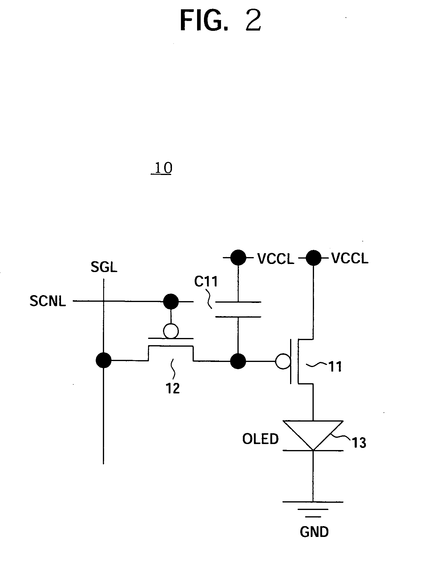
[0100]FIG. 9 is a circuit diagram of an active matrix type organic EL display (display device) according to a first embodiment of the present invention. Further, FIG. 10 is a diagram of a layout of power supply lines of the active matrix type organic EL display according to the first embodiment.

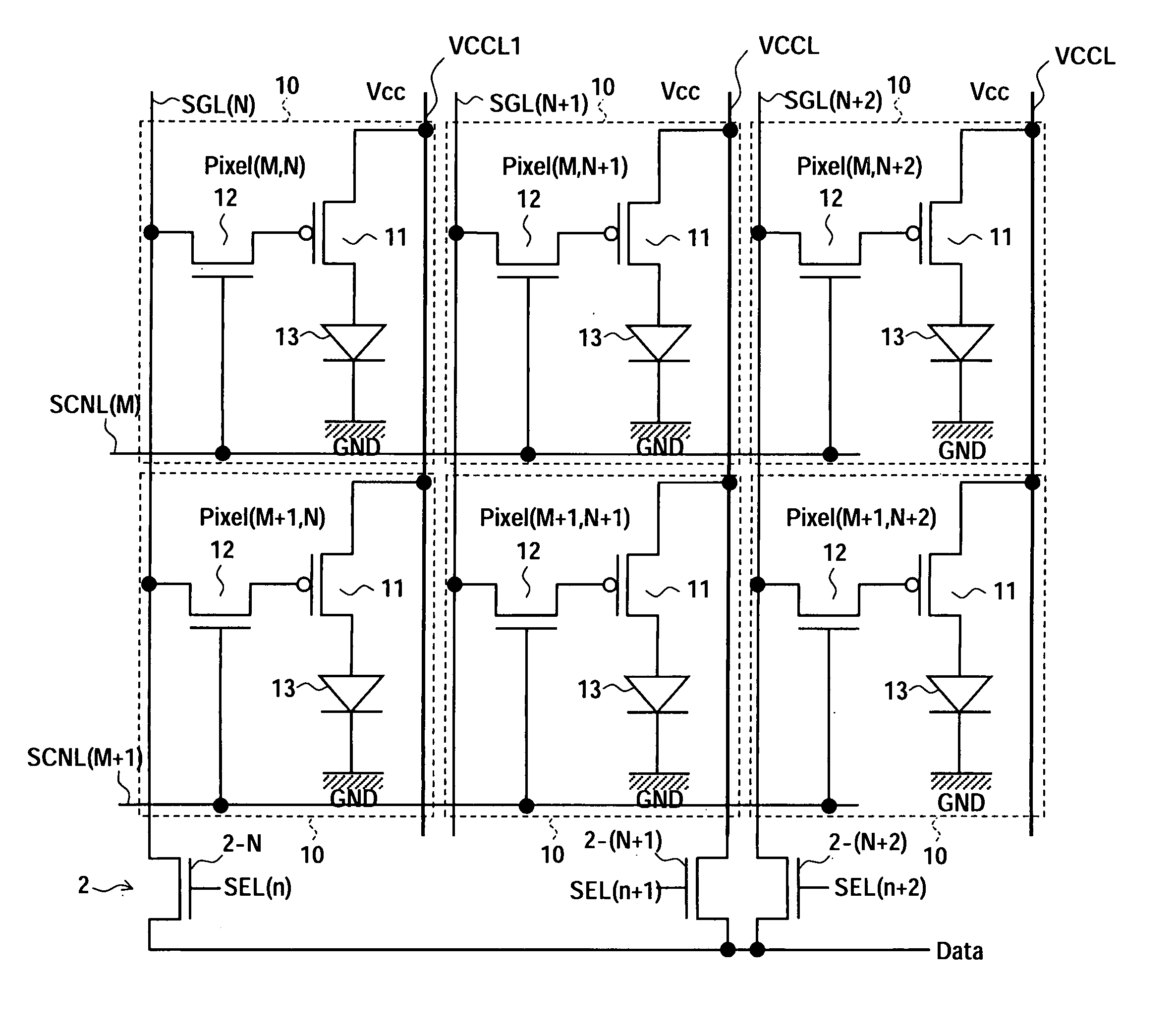
[0101] The present organic EL display 100 has, as shown in FIG. 9, a pixel array 102 including pixel circuits 101 arranged in an m×n matrix, a data driver (DDRV) 103, and a scan driver (SDRV) 104. n number of columns' worth of signal lines SGL1 to SGLn driven by the data driver (DDRV) 103 are arranged for each pixel column of the matrix array of the pixel circuits 101, while m number of rows' worth of scanning lines SCNL101 to SCNL10m selectively driven by the data driver (SDRV) 104 are arranged for each pixel row.

[0102] Further, in the present embodiment, the power supply potential lines VCCL, as shown in FIG. 10, are made common at the top and bottom of the display region constituted by t...

second embodiment

[0119]FIG. 11 is a circuit diagram of an active matrix type organic EL display device (display device) according to a second embodiment of the present invention. Further, FIG. 12 is a diagram of the layout of the power supply lines of an active matrix type organic EL display device according to the second embodiment.

[0120] The organic EL display 100A has, as shown in FIG. 11, a pixel array 102A including pixel circuits 101A arranged in an m×n matrix, a data driver (DDRV) 103, and a scan driver (SDRV) 104A. Further, the n number of columns' worth of the signal lines SGLL to SGLn driven by the data driver (DDRV) 103 are arranged for each pixel column of the matrix array of the pixel circuits 101A, and m number of rows' worth of the scanning lines SCNL101 to SCNL10m, drive lines DRL101 to DRL10m, and auto zero lines AZL101 to AZL10m selectively driven by the scan driver (SDRV) 104A are arranged for each pixel row.

[0121] Further, in the present embodiment, n number of columns' worth o...

third embodiment

[0147]FIG. 13 is a circuit diagram of an active matrix type organic EL display device (display device) according to a third embodiment of the present invention.

[0148] The difference of the third embodiment from the second embodiment resides in the configuration of a pixel circuit 101B. Below, an explanation will be given of the configuration and the operation of a pixel circuit 101B according to the third embodiment.

[0149] Each of the pixel circuits 101B according to the third embodiment has, as shown in FIG. 13, a p-channel TFT 121, n-channel TFT 122 to TFT 125, capacitors C121 and C122, a light emitting element 126 made of an organic EL element OLED (electrooptic element) 126, and nodes ND121 to ND123. Among these components, TFT 121 forms the field effect transistor, TFT 122 forms the first switch, TFT 123 forms the second switch, TFT 125 forms the third switch, TFT 124 forms the fourth switch, and the capacitor C121 forms the capacitor of the present invention. Further, the sc...


PUM


Abstract

A display device having at least a plurality of pixel circuits, connected to signal lines to which data signals in accordance with luminance information are supplied, arranged in a matrix, wherein pixel circuits of odd number columns and even number columns adjacent sandwiching an axis in a column direction parallel to an arrangement direction of the signal lines have a mirror type circuit arrangement symmetric about the axis of the column direction, and there are lines different from the signal lines between signal lines of adjacent pixel circuits.

Description

CROSS REFERENCES TO RELATED APPLICATIONS [0001] The present invention contains subject matter related to Japanese Patent Applications No. 2004-159378 and No. 2004-159379 filed in the Japan Patent Office on May 28, 2004, the entire contents of which being incorporated herein by reference. BACKGROUND OF THE INVENTION [0002] 1. Field of the Invention [0003] The present invention relates to a pixel circuit having an electrooptic element controlled in luminance by a signal line in an organic electroluminescence (EL) display device, liquid crystal display (LCD) device, or other active matrix display device and an interconnect structure and arrangement and circuit in an image display device in which these pixel circuits are arranged in a matrix. [0004] 2. Description of the Related Art [0005] In an active matrix type display device, use is made of electrooptic elements such as liquid crystal cells and organic EL elements as display elements of pixels. Among them, an organic EL element has ...

Claims


Application Information

Patent Timeline
Patent Type & Authority Applications(United States)
IPC IPC(8): G09G3/30G09G3/32G09G3/36
CPCG09G3/3233H01L27/3276G09G2300/0426G09G2300/0443G09G2300/0819G09G2300/0852G09G2300/0861G09G2300/0866G09G2310/061G09G2320/0209G09G2330/021G09G5/00G09G3/325G09G2310/0251H01L27/3262H01L27/3265G09G3/3648H01L29/42384H01L29/78645G09G3/30G09G3/3611G09G5/18G09G2300/0404H10K59/123H10K59/131H10K59/1213H10K59/1216H01L27/124
Inventor ASANO, MITSURU
Owner SONY CORP
Why Eureka
Try Eureka