Shift resistor circuit and method of operating the same

a resistor circuit and resistor technology, applied in logic circuits, digital storage, instruments, etc., can solve the problems of increasing manufacturing costs, difficult to implement a high resolution lcd device using amorphous silicon tft, and low mobility of amorphous silicon tft, so as to reduce the driving load of the module and reduce the consumption of electric power

Active Publication Date: 2005-12-01
LG DISPLAY CO LTD
View PDF4 Cites 17 Cited by
  • Summary
  • Abstract
  • Description
  • Claims
  • Application Information

AI Technical Summary

Benefits of technology

[0027] An advantage of the present invention is to provide a shift resistor circuit that consumes less electric power by using a clock signal having a low swing voltage inputted from an external circuit in order to reduce a driving load in a module, and a method of operating thereof.
[0028] Additional advantages and features of the invention will be set forth in part in the description which follows and in part will become apparent to those having ordinary skill in the art upon examination of the following or may be learned from practice of the invention. These and other advantages of the invention may be realized and attained by the structure particularly pointed out in the written description and claims hereof as well as the appended drawings.
[0029] To achieve these and other advantages and in accordance with the present invention, as embodied and broadly described herein, a shift resistor circuit includes an OR-gate unit for receiving a start pulse or an output of a previous stage and a feedback signal; a level shift unit for level-shifting a swing voltage of a clock signal in response to an output signal of the OR-gate unit; and a buffer for transferring an output of the level shift unit to a next stage as an input signal.
[0030] In another aspect of the present invention, a method of operating a shift resistor circuit includes inputting a start pulse or an output of a previous stage and a feedback signal to an OR-gate unit; defining an operating period by an output signal of the OR-gate unit and level-shifting a swing voltage of a clock signal by a level shift unit; and transferring an output of the level shift unit to a next state using a buffer.
[0031] In yet another aspect of the present invention, a display device includes an image display unit for displaying images and a control chip for generating a clock signal; and a shift register circuit electrically connected to the image display unit and the control chip, the shift register circuit including a level shift unit for level-shifting a swing voltage of the clock signal.

Problems solved by technology

However, it is difficult to implement an LCD device with a high resolution using the amorphous silicon TFT because the mobility of the amorphous silicon TFT is comparatively low.
In other words, when the amorphous silicon TFT is used for manufacturing an LCD device, peripheral driving circuits such as the gate driver and the data driver should be separately manufactured and installed into the LCD device, which increases the manufacturing cost.
However, manufacturing a LCD panel using the CMOS TFT requires many processes, thereby increasing the manufacturing cost and degrading the reliability.
However, it is generally difficult to generate such a clock signal having a swing width greater than 10V including a negative voltage using an external chip such as the control chip 22.
In other words, it is difficult to manufacture an integrated chip that can generate a clock signal having a swing width greater than 10 V or a negative voltage.

Method used


Image

  • Shift resistor circuit and method of operating the same
  • Shift resistor circuit and method of operating the same
  • Shift resistor circuit and method of operating the same

Examples


Embodiment Construction

[0041] Reference will now be made in detail to embodiments of the present invention, examples of which are illustrated in the accompanying drawings. Wherever possible, the same reference numbers will be used throughout the drawings to refer to the same or like parts.

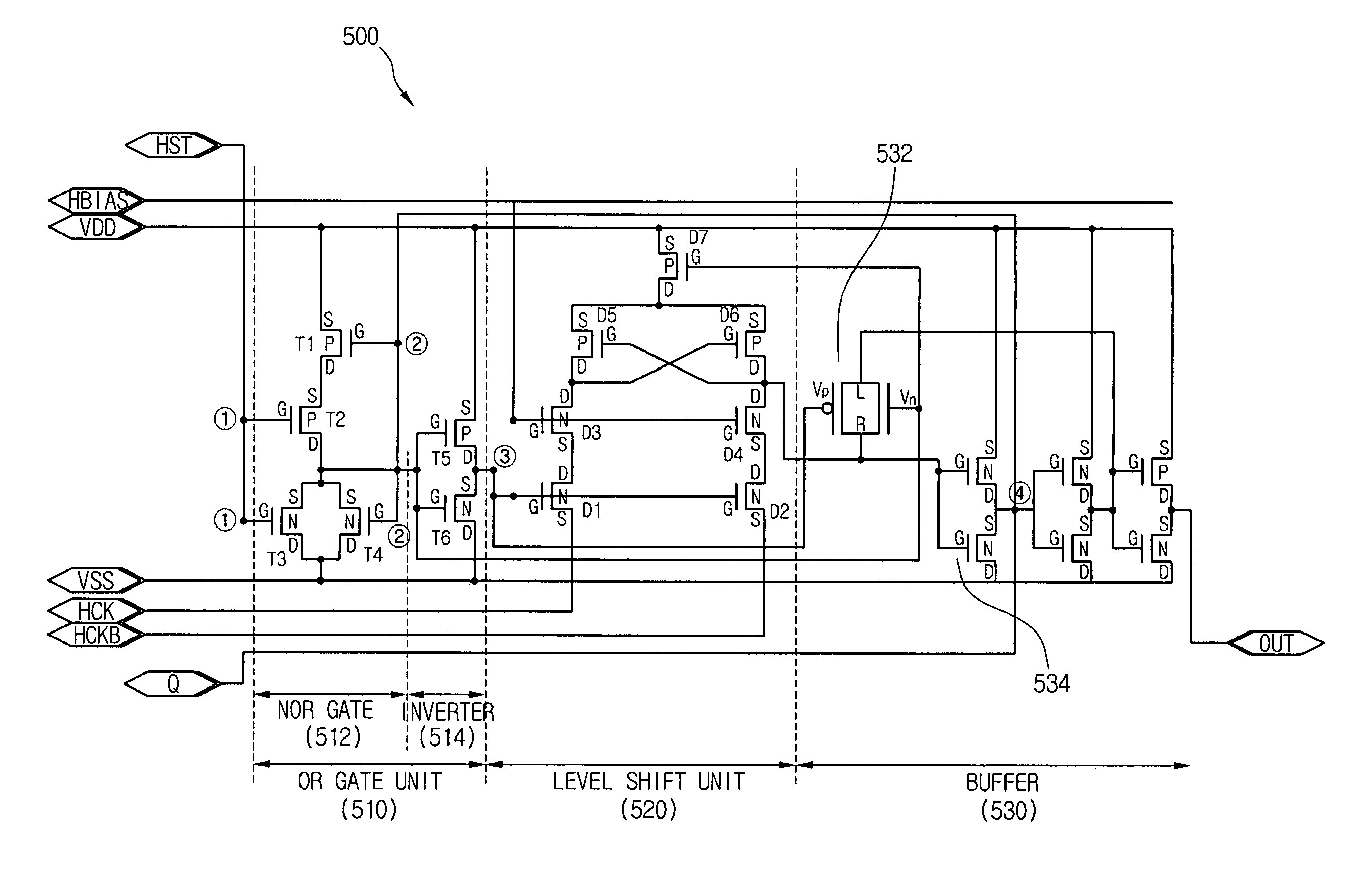
[0042]FIG. 4 is a block diagram illustrating a shift resistor according to an embodiment of the present invention.

[0043] As illustrated in FIG. 4, the shift resistor includes a plurality of stages, each of which is connected to two-phase clock signal supplying lines HCK, HCKB. Each of the stages sequentially generates a sampling signal by shifting a predetermined input signal. That is, a first stage ST1 receives a start pulse HST and each of a second to nth stages ST2 to STn receives an output signal of the previous stage.

[0044] In more detail, the plurality of stages ST1 to STn are dependently connected to a start pulse input line and each stage is connected to the two-phase clock signal supplying lines HCK, HCKB. Th...


PUM


Abstract

A shit resistor circuit and a method of operating the same are disclosed. The shift resistor circuit includes an OR-gate unit for receiving a start pulse or an output of a previous stage and a feedback signal; a level shift unit for level-shifting a swing voltage of a clock signal in response to an output signal of the OR-gate unit; and a buffer for transferring an output of the level shift unit to a next stage as an input signal.

Description

[0001] This application claims the benefit of Korean Patent Application No. 2004-38847, filed on May 31, 2004, which is hereby incorporated by reference for all purposes as if fully set forth herein. BACKGROUND OF THE INVENTION [0002] 1. Field of the Invention [0003] The present invention relates to a shift resistor circuit, and more particularly, to a shift resistor circuit in a driving circuit for a liquid crystal display device and a method of operating the same. [0004] 2. Discussion of the Related Art [0005] Liquid crystal display (LCD) devices display images by controlling an amount of light passing through a liquid crystal layer using an electric field. An LCD device includes a liquid crystal display (LCD) panel having a plurality of liquid crystal cells arranged in a matrix configuration and a driving circuit to drive the LCD panel. [0006] The LCD panel includes gate lines and data lines crossing each other, and the liquid crystal cells are arranged near the crossing points o...

Claims


Application Information

Patent Timeline
Patent Type & Authority Applications(United States)
IPC IPC(8): G09G3/36G11C19/28H03K19/00
CPCG09G3/3674G11C19/28G09G2310/0289G09G3/3685G09G3/36H03K19/00
Inventor LIM, KYOUNG MOON
Owner LG DISPLAY CO LTD
Why Eureka
Try Eureka