Method for fabricating capacitor

a capacitor and capacitor technology, applied in the field of semiconductor devices, can solve the problems of difficult fabrication of stable high-k dielectric films on the lower electrodes, the miniaturization of integrated circuits, etc., and achieve the effect of not increasing the total reducing the number of fabricating steps, and reducing the size of the capacitor

Inactive Publication Date: 2005-12-01
UNITED MICROELECTRONICS CORP
View PDF4 Cites 8 Cited by
  • Summary
  • Abstract
  • Description
  • Claims
  • Application Information

AI Technical Summary

Benefits of technology

[0009] The integrated capacitor and interconnect process of this invention is the combination of the above method and an interconnect process. Specifically, a metal wiring line is formed together with the metal layer, and a via hole exposing a portion of the metal wiring line is formed in the insulating layer together with the opening exposing a portion of the metal layer. The width of the via hole is smaller than that of the opening, so that a metal plug can be formed in the via hole simultaneously with formation of the metal spacer on the sidewall of the opening. Then, an upper wiring line is formed together with the upper electrode to connect with the metal plug.
[0010] Since the lower electrode of the capacitor made with the above method includes at least one metal spacer, the inter-electrode area of the capacitor can be increased in the vertical direction to provide larger capacitance. In other words, the capacitor takes a smaller lateral area as compared with a conventional MIM capacitor that provides the same capacitance. Moreover, the method for fabricating a capacitor can be integrated with an interconnect process, so that the total number of fabricating steps is not increased.

Problems solved by technology

Though the capacitance limitation can be overcome by increasing the lateral area of the MIM capacitor, such a solution inevitably prevents miniaturization of the integrated circuits.
Moreover, increasing the dielectric constant of the insulator between the lower and upper electrodes can also increase the capacitance, but fabricating a stable high-k dielectric film on the lower electrode is not so easy.

Method used


Image

  • Method for fabricating capacitor
  • Method for fabricating capacitor
  • Method for fabricating capacitor

Examples


Embodiment Construction

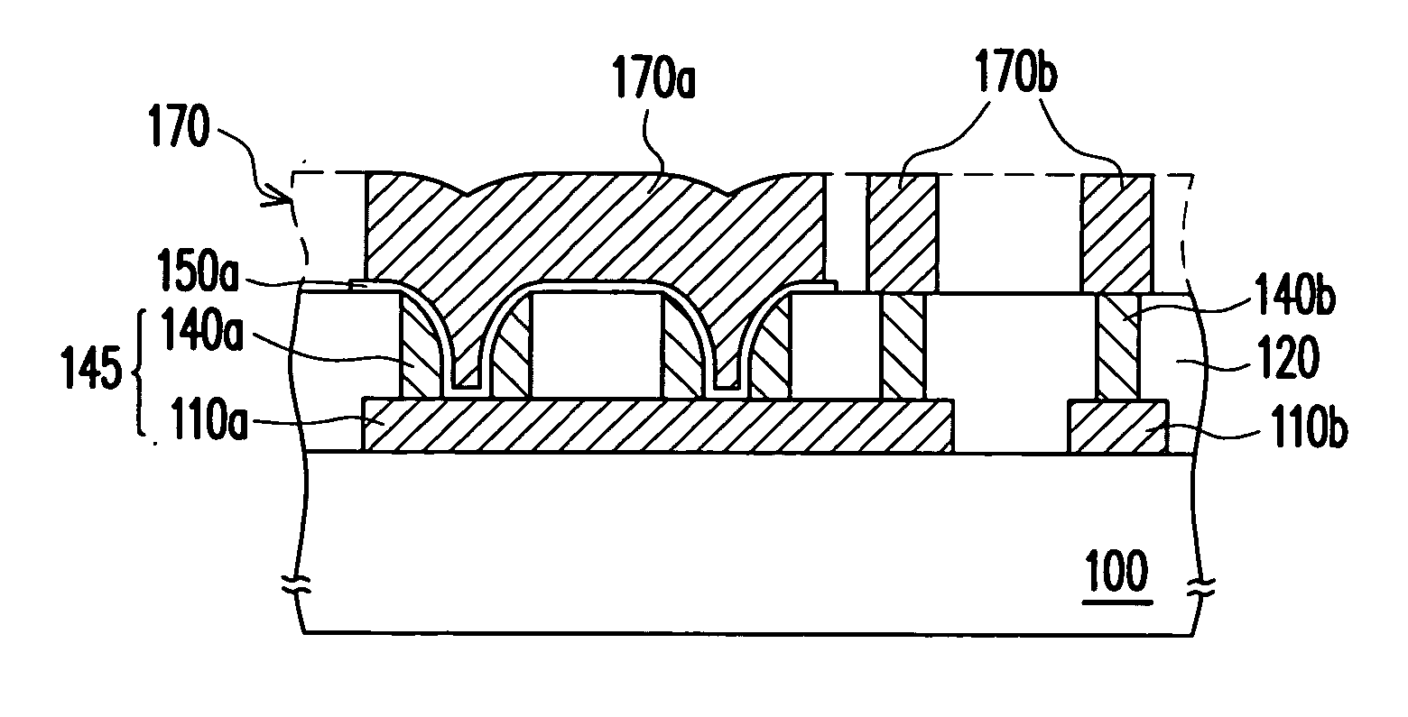
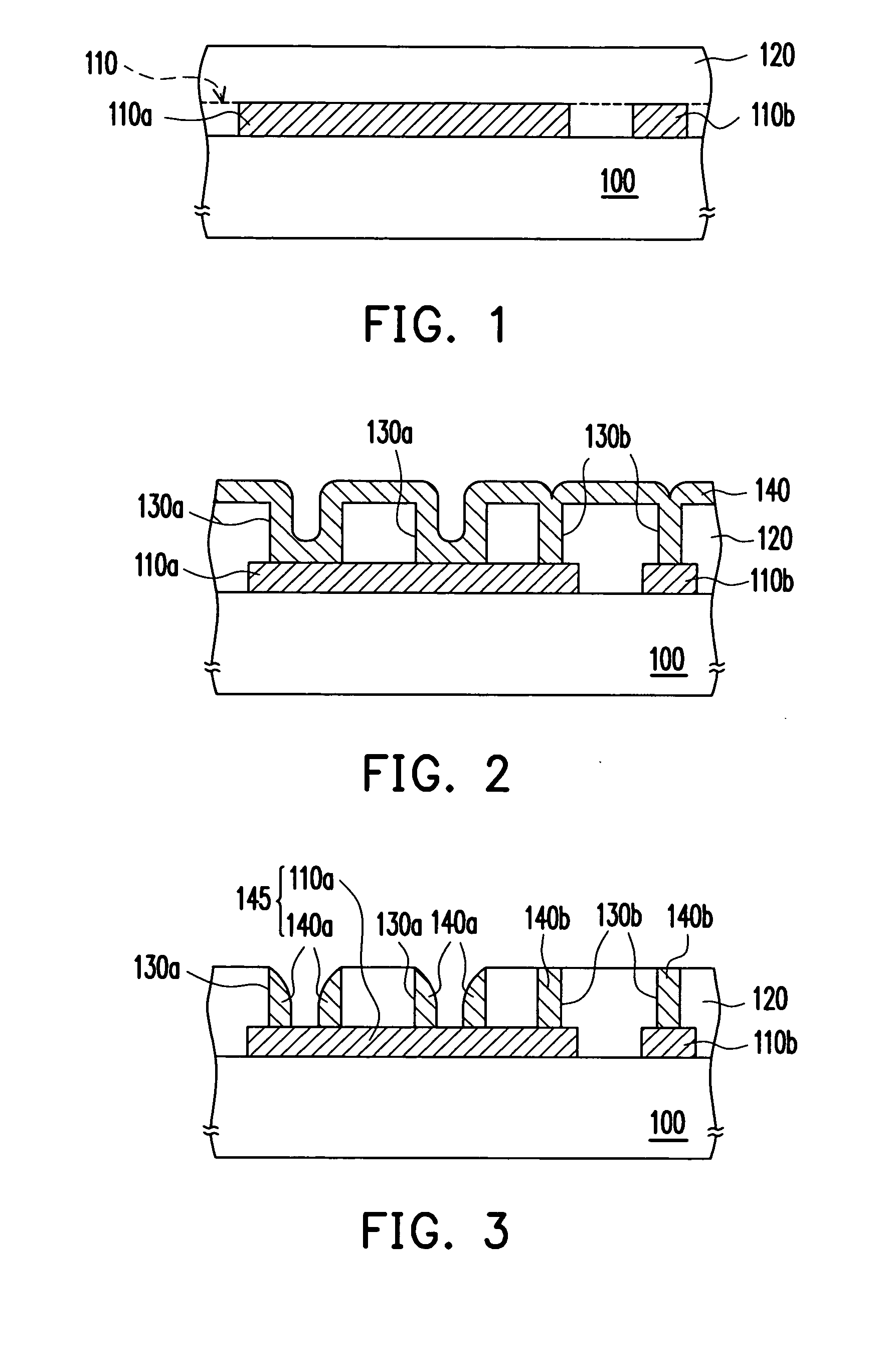
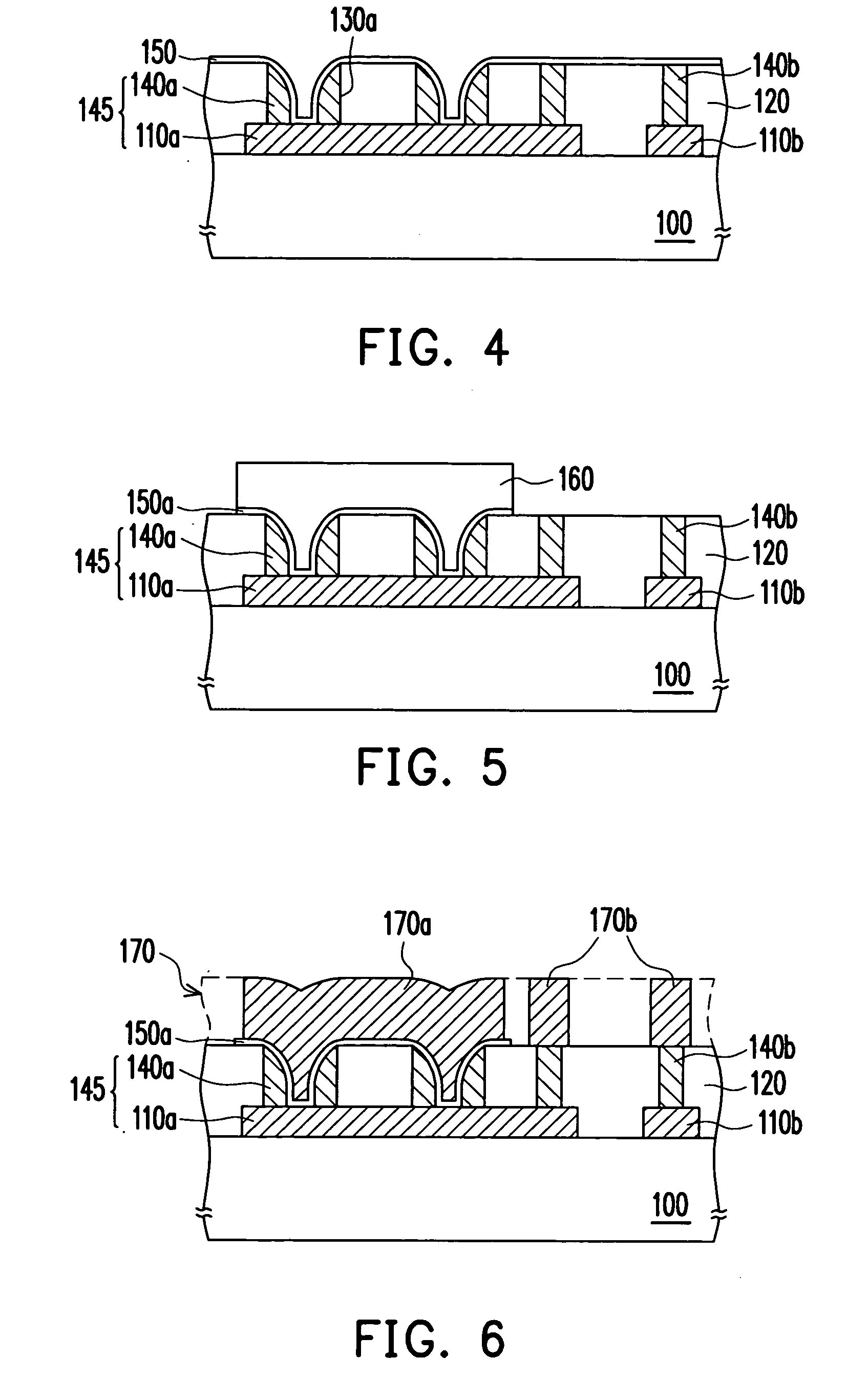
[0014] Referring to FIG. 1, a substrate 100 is provided, which may be a semiconductor substrate formed with semiconductor devices and interconnect structures thereon. A metal layer 110 is formed on the substrate 100, and then patterned into a lower electrode base plate 110a and a wiring line 110b. The material of the metal layer 110 is selected from the group consisting of Al, Cu, Ti, Ta, Mo and combinations thereof. Then, an intermetal dielectric (IMD) layer 120 is formed over the substrate 100 covering the lower electrode base plate 110a and the wiring line 110b. The EMD layer 120 may be further planarized if it is not formed to have a planar top surface. The material of the IMD layer 120 can be SiO2 or a low-k material like FSG, aerogel, SILK or FLARE.

[0015] Referring to FIG. 2, openings 130a and via holes 130b are simultaneously formed in the insulating layer 120, wherein the openings 130a expose portions of the lower electrode base plate 110a, a via hole 130b exposes another p...


PUM

PropertyMeasurementUnit
widthaaaaaaaaaa
thicknessaaaaaaaaaa
dielectricaaaaaaaaaa

Abstract

A method for fabricating a capacitor is described. A metal layer is formed on a substrate, and then an insulating layer is formed over the substrate covering the metal layer. At least one opening is formed in the insulating layer exposing a portion of the metal layer, and a metal spacer is formed on the sidewall of the opening, wherein the metal spacer and the metal layer together constitute a lower electrode. A dielectric layer is formed on the lower electrode, and then an upper electrode is formed on the dielectric layer.

Description

BACKGROUND OF THE INVENTION [0001] 1. Field of the Invention [0002] The present invention relates to a semiconductor process. More particularly, the present invention relates to a method for fabricating a capacitor, and an integrated capacitor and interconnect process based on the same method. [0003] 2. Description of the Related Art [0004] MIM (metal / insulator / metal) capacitors are widely applied in mixed-mode or RF integrated circuits, and therefore take a large proportion of the lateral area in them. A conventional MIM capacitor is fabricated by sequentially stacking a first metal layer, a dielectric layer and a second metal layer on the substrate. The first metal layer, i.e., the lower electrode, usually has a planar shape so that the capacitance of the MIM capacitor is limited. [0005] Though the capacitance limitation can be overcome by increasing the lateral area of the MIM capacitor, such a solution inevitably prevents miniaturization of the integrated circuits. Moreover, inc...

Claims


Application Information

Patent Timeline
Patent Type & Authority Applications(United States)
IPC IPC(8): H01L21/02H01L21/44H01L21/8234H01L27/08
CPCH01L28/91H01L27/0805
Inventor GAU, JING-HORNG
Owner UNITED MICROELECTRONICS CORP
Why Eureka
Try Eureka