Method of growing semiconductor nanowires with uniform cross-sectional area using chemical vapor deposition

a technology of chemical vapor deposition and semiconductor nanowires, which is applied in the direction of nanoinformatics, polycrystalline material growth, crystal growth process, etc., can solve the problems of non-uniform cross-sectional area, significant taper of nanowires, and unsuitability for us

Inactive Publication Date: 2005-12-01
AGILENT TECH INC
View PDF2 Cites 65 Cited by
  • Summary
  • Abstract
  • Description
  • Claims
  • Application Information

AI Technical Summary

Benefits of technology

[0009] Removing the adatoms of the constituent element from the lateral surface of the nanowire as the nanowire is grown and before such adatoms are incorporated into the n

Problems solved by technology

However, attempts to grow nanowires by MOCVD have typically yielded nanowires that taper significantly.
Such nanowires therefore have non-uniform cross-sectional areas and are therefore unsuitable for use in applications that need nanowires with a uniform c

Method used


Image

  • Method of growing semiconductor nanowires with uniform cross-sectional area using chemical vapor deposition
  • Method of growing semiconductor nanowires with uniform cross-sectional area using chemical vapor deposition
  • Method of growing semiconductor nanowires with uniform cross-sectional area using chemical vapor deposition

Examples


Embodiment Construction

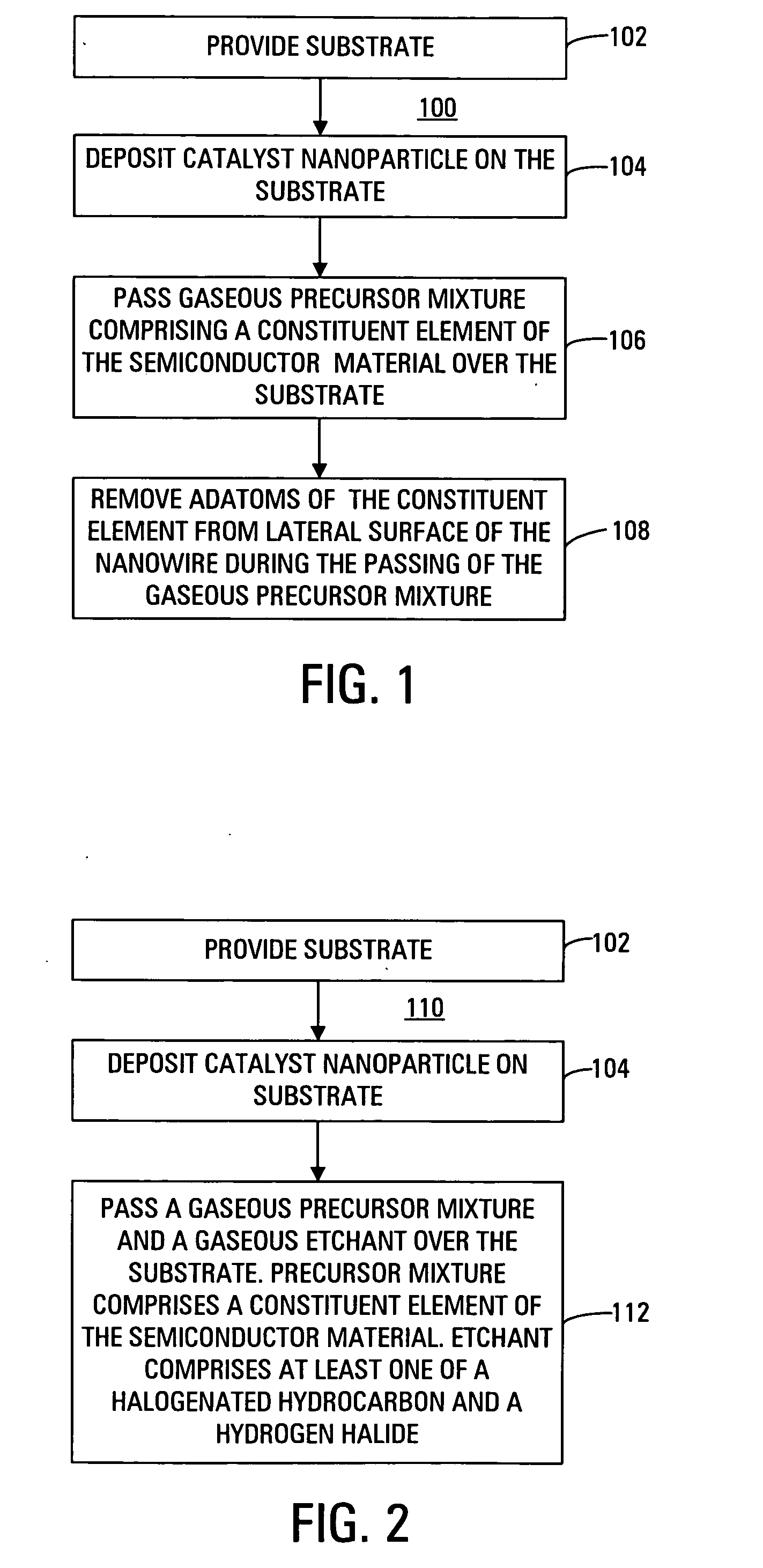
[0018]FIG. 1 is a flow chart illustrating a first embodiment 100 of a method in accordance with the invention for using a chemical vapor deposition (CVD) process such as metal-organic chemical vapor deposition (MOCVD) to grow a nanowire of a semiconductor material. The nanowire has a uniform cross-sectional area along its length.

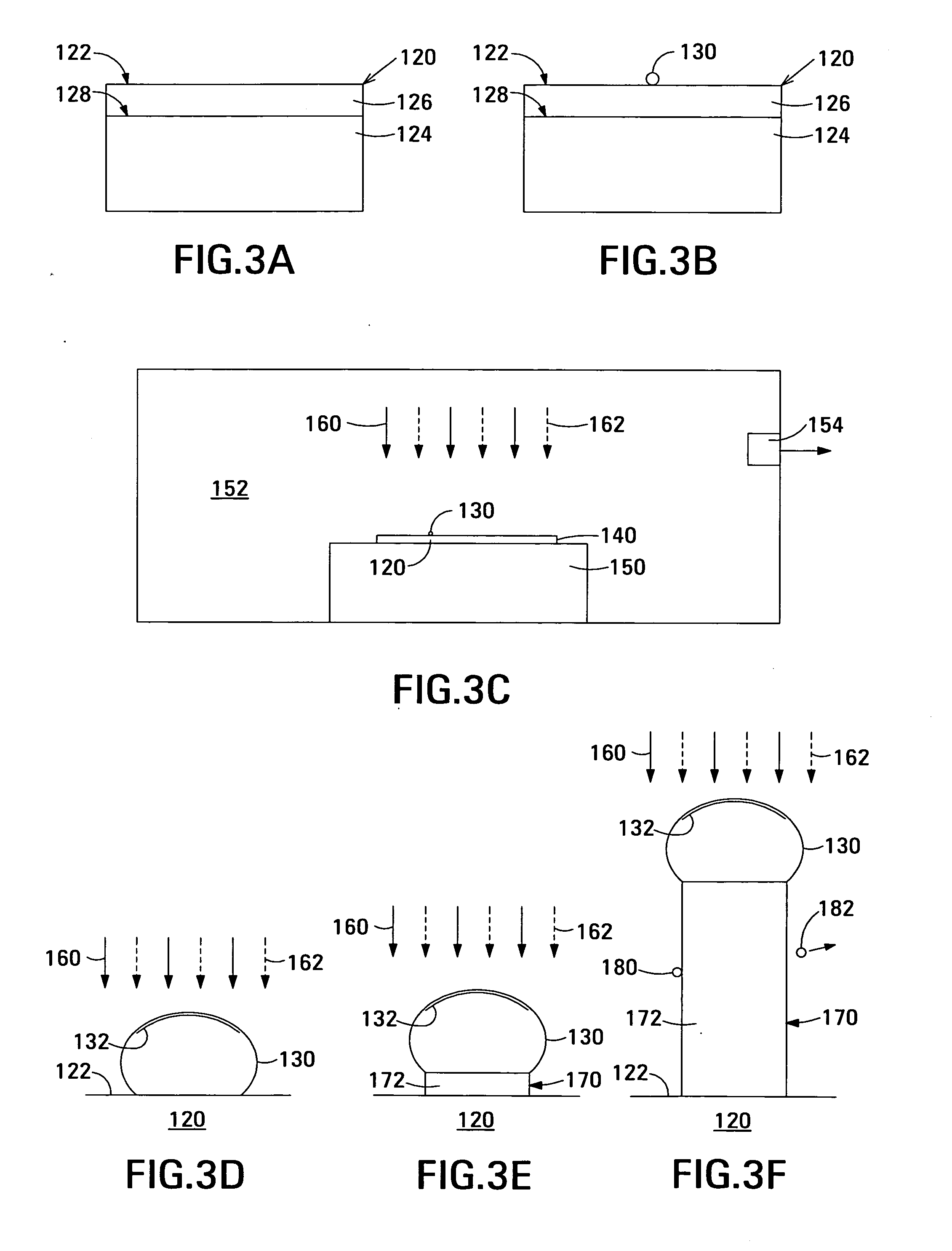
[0019] In block 102, a substrate is provided.

[0020] In block 104, a catalyst nanoparticle is deposited on the substrate.

[0021] In block 106, a gaseous precursor mixture comprising a constituent element of the semiconductor material of the nanowire is passed over the substrate.

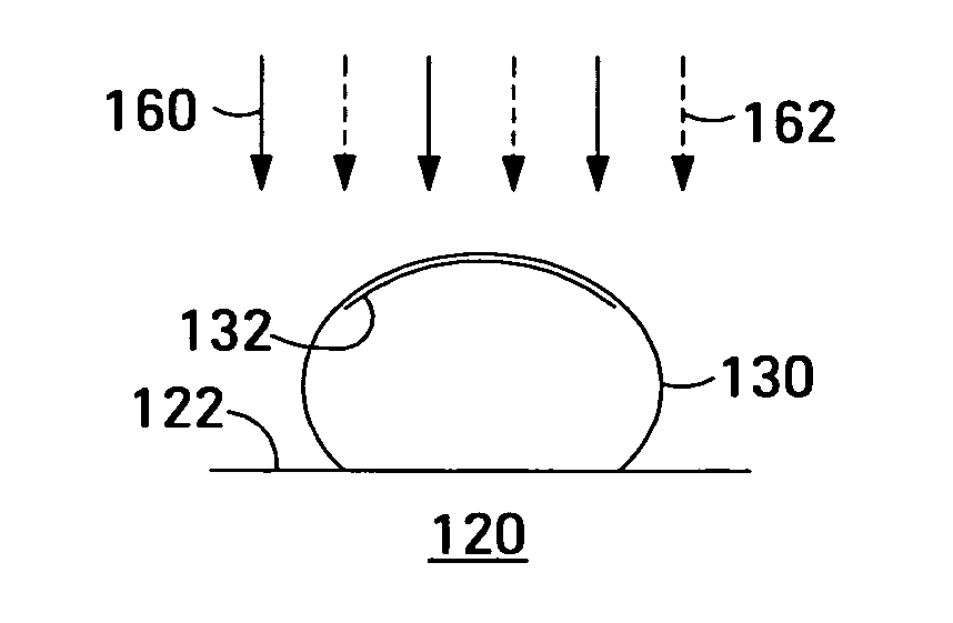
[0022] In block 108, adatoms of the constituent element are removed from a lateral surface of the nanowire during the passing of the precursor mixture.

[0023] In an embodiment, in block 108, the adatoms of the constituent element are removed by additionally passing a gaseous etchant over the substrate.

[0024] In another embodiment, in block 108, the adatoms of the constituent elemen...


PUM


Abstract

A nanowire of a semiconductor material and having a uniform cross-sectional area along its length is grown using a chemical vapor deposition process. In the method, a substrate is provided, a catalyst nanoparticle is deposited on the substrate, a gaseous precursor mixture comprising a constituent element of the semiconductor material is passed over the substrate, and adatoms of the constituent element are removed from a lateral surface of the nanowire during the passing of the precursor mixture. Removing the adatoms of the constituent element before such adatoms are incorporated into the nanowire prevents such adatoms from accumulating on the lateral surface of the nanowire and allows the nanowire to grow with a uniform cross-sectional area along its length.

Description

BACKGROUND [0001] Semiconductor nanowires are elongate structures having at least one dimension in the range from about 1 nm and 100 nm. Nanowires are nanoscale building blocks useable in such applications as nanoscale electronic devices and nanoscale photonic devices. Semiconductor nanowires allow such devices to be fabricated without the need for advanced lithographic techniques. The electrical and optical properties of the nanowires are strongly affected by the nanowires' diameter and cross-sectional shape. Some applications require the synthesis of nanowires with well-controlled diameters and cross-sectional shapes. [0002] A number of different methods have been used to grow semiconductor nanowires. Some of the available methods are described by Younan Xia et al. in One-Dimensional Nanostructures: Synthesis, Characterization and Applications, 15 ADV. MATER. 353-389 (March 2003). Vapor-liquid-solid (VLS) growth is one method widely used to synthesize nanowires. A typical VLS proc...

Claims


Application Information

Patent Timeline
IPC IPC(8): C30B11/12C30B29/06C30B29/42C30B29/60H01L21/20H01L21/205H01L21/36
CPCB82Y10/00Y10S977/818C30B11/12C30B29/06C30B29/42C30B29/605H01L21/0237H01L21/02488H01L21/02543H01L21/02546H01L21/02603H01L21/0262H01L21/02645H01L21/02653Y10S977/762B82Y30/00
Inventor YI, SUNG SOO
Owner AGILENT TECH INC
Why Eureka
Try Eureka