Method of patterning wall and phosphor well matrix utilizing glass

a technology of phosphor well matrix and patterning wall, which is applied in the manufacture of electrode systems, cold cathode manufacturing, and electric discharge tube/lamp manufacture, etc. it can solve the problems of requiring yet more power for backlighting, affecting the quality of fpds, and the difficulty of adjusting the pixel switching element, so as to reduce the emitted outgasses, increase the reflective properties, and increase the effect of luminous efficiency

Inactive Publication Date: 2005-12-08
CANON KK
View PDF20 Cites 0 Cited by
  • Summary
  • Abstract
  • Description
  • Claims
  • Application Information

AI Technical Summary

Benefits of technology

[0013] Accordingly, the present invention provides a support structure that provides a reduction in emitted outgasses during display operation. The present invention further provides a support structure which achieves the above listed accomplishment and which further provides increased reflective properties so as to provide greater luminous efficiency. The present invention additionally provides a support structure that achieves the above listed accomplishments and which is less costly to manufacture. The present invention further provides a support structure that achieves the above listed accomplishments and which is etchable. The present invention further provides a support structure that achieves the above listed accomplishments and which further provides a method of etching which is clean, inexpensive, highly accurate and which does not adversely affect the substrate upon which the support structure is disposed.

Problems solved by technology

For example, neither LCDs or AMLCDs can provide adequate viewing when viewed from an off-center angle, and they require backlighting which requires yet more power.
TFTs are subject to immense quality control difficulties associated with each pixel's switching element, produced using integrated circuit techniques.
Further, most FPDs cost substantially more than a CRT of an equivalent size.
In fact, none of the FPDs or CRTs have been able to meet all of the needs for improving power consumption, increasing brightness efficiency, increased video response, improved viewing angles, cooler operating temperatures, providing full color range, scaleability, ruggedness, and packaging.
Further, the support structures must be relatively easy to manufacture and cost effective, or risk having an overly expensive display product price, effectively reducing possible market share.
Unfortunately, polymers such as polyimides and polyamides are prone to excessive gas emissions during tube operation, such that even after outgassing, they are well known in the art to continue to generate gas within the display tube upon electron bombardment during display operation.
This continual generation of gas during display operation causes a reduction of display performance and also reduces the approximated lifespan of the display device.
Additionally, the polymers, (polyimides and polyamides) are very expensive, both in raw materials and in the processing costs related to the construction of the wall supports.
Further, these materials have a low reflective index, which reduces the overall performance of the display, and they exhibit poor electrical conductivity.
Unfortunately, current sandblasting techniques are not without drawbacks, e.g., the residue of the sandblasting is difficult to contain, it is very difficult to stop erosion at the material / substrate interface without inadvertent sandblasting of the substrate, it is slow and therefore costly, and the precision of the sandblasting is predicated upon the grit size of the sand, which is commonly around ten microns.

Method used


Image

  • Method of patterning wall and phosphor well matrix utilizing glass
  • Method of patterning wall and phosphor well matrix utilizing glass
  • Method of patterning wall and phosphor well matrix utilizing glass

Examples


Embodiment Construction

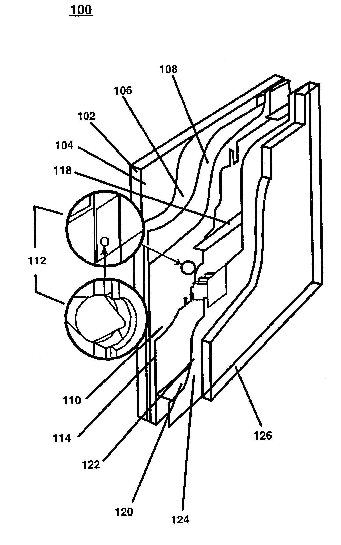
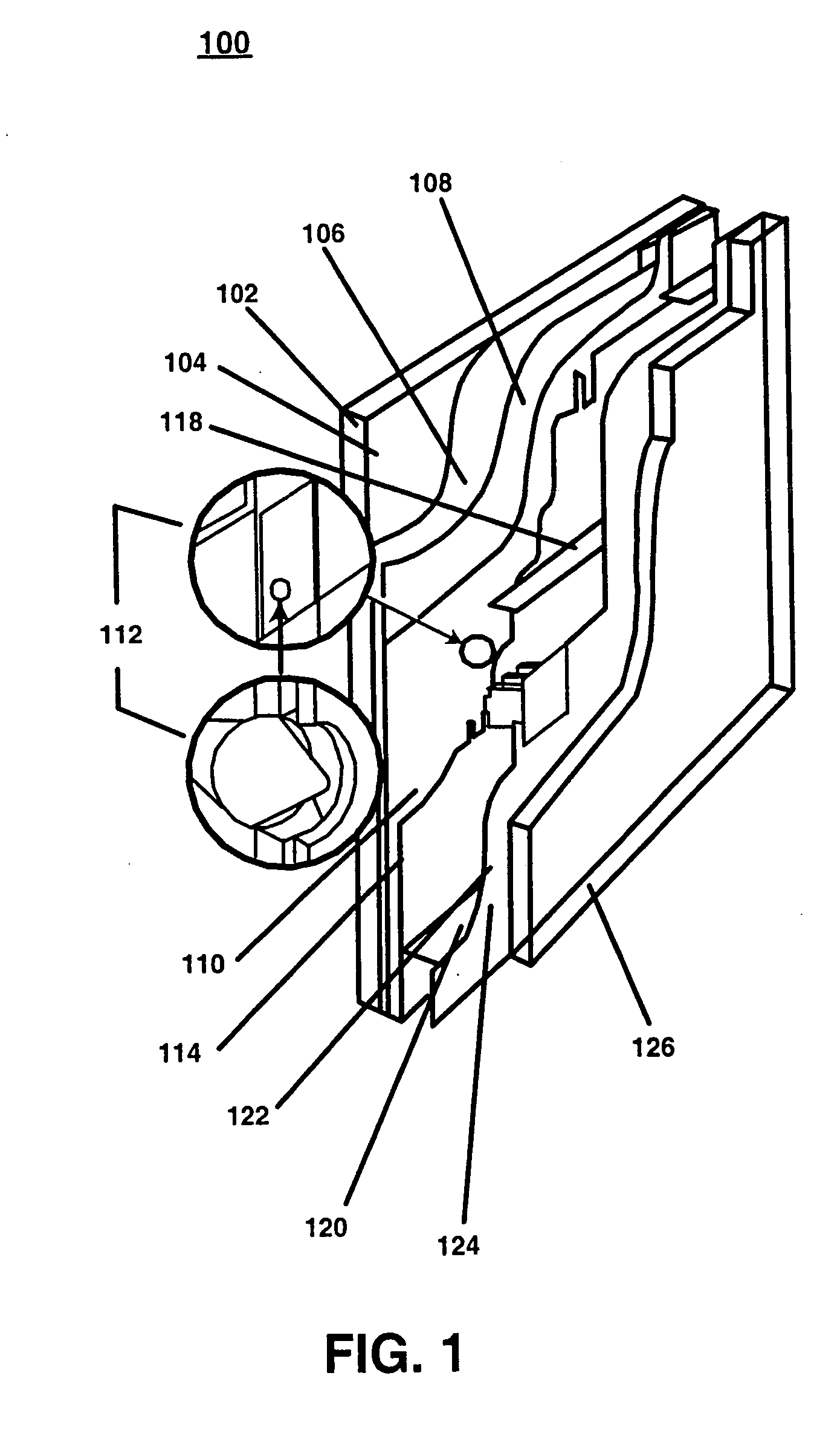
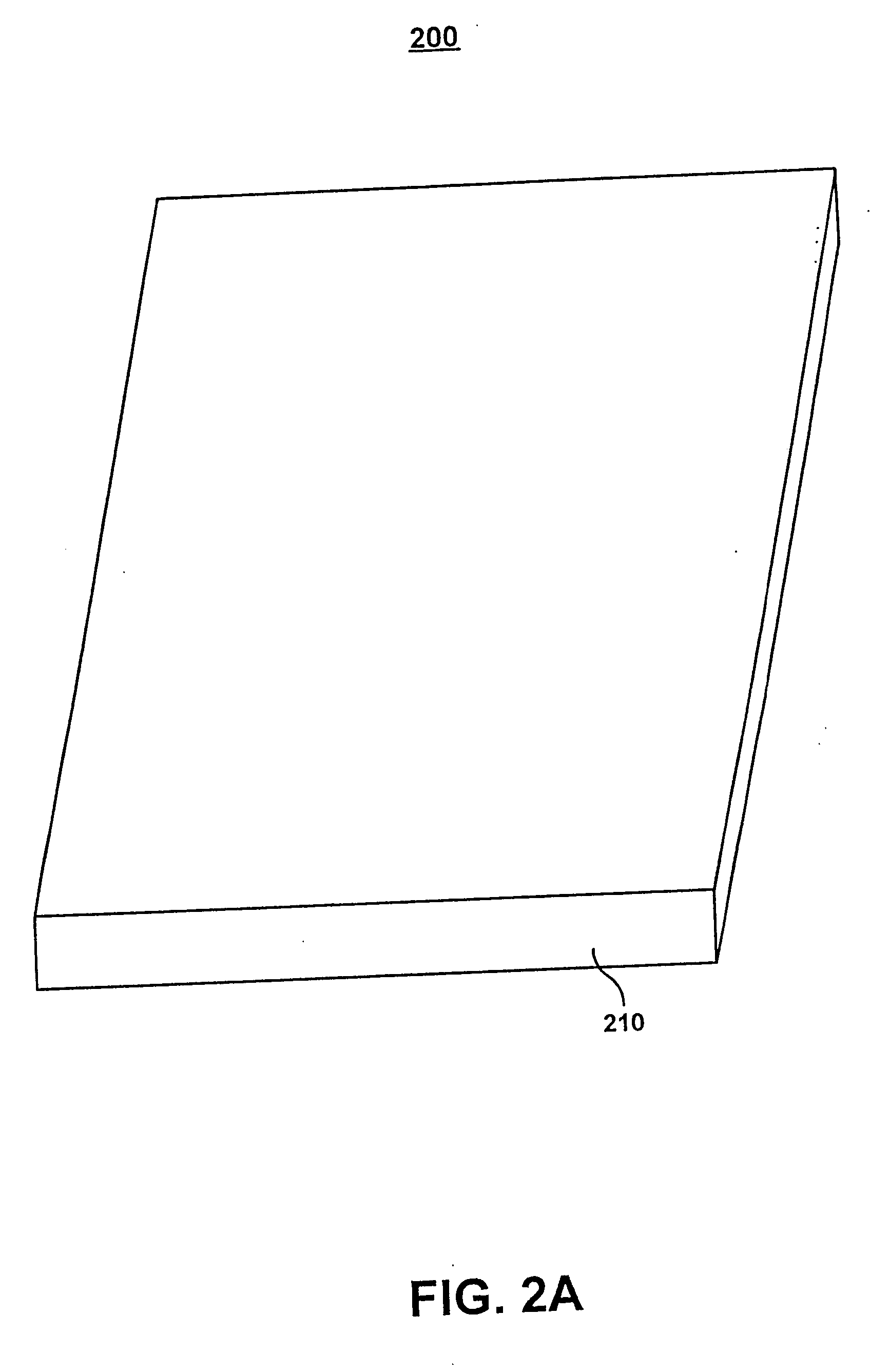
[0046] A method of fabricating a support structure utilizable in display device assembly is described. In the following description, for purposes of explanation, numerous specific details are set forth in order to provide a thorough understanding of the present invention. It will be obvious, however, to one skilled in the art that the present invention may be practiced without these specific details. In other instances, well-known structures and devices are shown in block diagram form in order to avoid obscuring the present invention.

[0047] Some portions of the detailed descriptions, which follow, are presented in terms of procedures, steps, processes, and other symbolic representations of operations concurrent with and implemented during the construction of a display device. These descriptions and representations are the means used by those skilled in the display device fabrication and processing arts to most effectively convey the substance of their work to others skilled in the ...


PUM

PropertyMeasurementUnit
sizeaaaaaaaaaa
thicknessaaaaaaaaaa
grit sizeaaaaaaaaaa

Abstract

A method of fabricating a support structure. In one embodiment, the method is comprised of forming a layer of material into the support structure. The layer of material is adapted to be attached onto a substrate surface. The method further comprises treating the layer of material. The present method is further comprised of etching said layer of material. The fabricated support structure is then implementable during assembly of a display device. In one embodiment, the support structure is attached to the substrate surface prior to the forming, treating, and etching of the layer of material. In another embodiment, the support structure is attached to the substrate surface subsequent to the forming, treating, and etching of the layer of material.

Description

CROSS REFERENCE TO RELATED APPLICATION [0001] This application is a Continuation-in-Part of co-pending U.S. patent application Ser. No. 09 / 970,051, attorney docket number CDST-C169, filed Oct. 2, 2001, by Theodore S. Fahlen, et al., and entitled “A METHOD OF FORMING POWDER METAL PHOSPHOR MATRIX AND GRIPPER STRUCTURES IN WALL SUPPORT.”BACKGROUND OF THE INVENTION [0002] 1. Field of the Invention [0003] The present invention relates to display device fabrication. More particularly, the present invention relates to the technology and fabrication of flat panel displays, e.g., field emission displays. [0004] 2. Related Art [0005] Advancements in electronics and computer display technologies have created new categories of display devices as well as enabling improvements upon existing display technologies. New categories of display devices include FPDs, (flat panel displays), e.g., TFTs (thin film technology), LCDs (liquid crystal display), AMLCDs (active matrix liquid crystal display), and...

Claims


Application Information

Patent Timeline
Patent Type & Authority Applications(United States)
IPC IPC(8): B23P25/00B32B17/10C03C17/00C03C17/36H01J9/24H01J29/70
CPCB32B17/10018Y10T29/49812C03C17/36C03C2217/40C03C2218/335H01J9/242H01J2211/36H01J2329/00H01J2329/8625Y10T29/49126Y10T29/49885Y10T29/49904Y10T29/4998Y10T29/49616C03C17/002
Inventor HOPPLE, GEORGE B.BARTON, ROGER W.PORTER, JOHN D.FAHLEN, THEODORE S.MACKEY, BOB L.
Owner CANON KK
Why Eureka
Try Eureka