Flip chip type nitride semiconductor light-emitting diode

a light-emitting diode and flip chip technology, applied in semiconductor devices, semiconductor/solid-state device details, electrical apparatus, etc., can solve the problems of reducing the light-emitting efficiency of the active layer, increasing the forward voltage, and reducing the luminance characteristics, so as to improve the p-electrode structure and low forward voltage. , the effect of high light-emitting efficiency

Active Publication Date: 2005-12-08
SAMSUNG ELECTRONICS CO LTD
View PDF4 Cites 59 Cited by
  • Summary
  • Abstract
  • Description
  • Claims
  • Application Information

AI Technical Summary

Benefits of technology

[0011] Therefore, the present invention has been made in view of the above problems, and it is an object of the present invention to provide a nitride semiconductor light-emitting diode having a relatively low forward voltage and high light-emitting efficiency by improving the p-electrode structure so as to alleviate the electric current crowding phenomenon.

Problems solved by technology

This electric current crowding not only increases a forward voltage, but also reduces light-emitting efficiency of the active layer spaced relative to the n-electrode, thereby decreasing luminance characteristics thereof.
In addition, the region A in which the electric current is concentrated has an increased heat value, thus significantly deteriorating reliability of the diode.

Method used


Image

  • Flip chip type nitride semiconductor light-emitting diode
  • Flip chip type nitride semiconductor light-emitting diode
  • Flip chip type nitride semiconductor light-emitting diode

Examples


Embodiment Construction

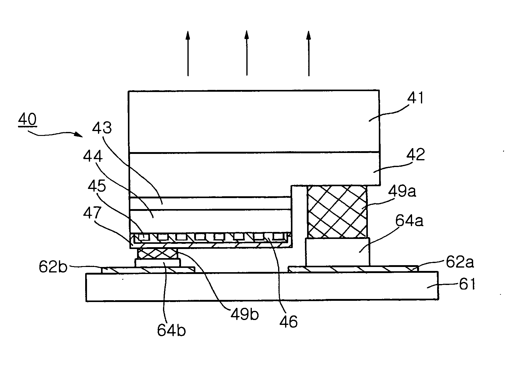
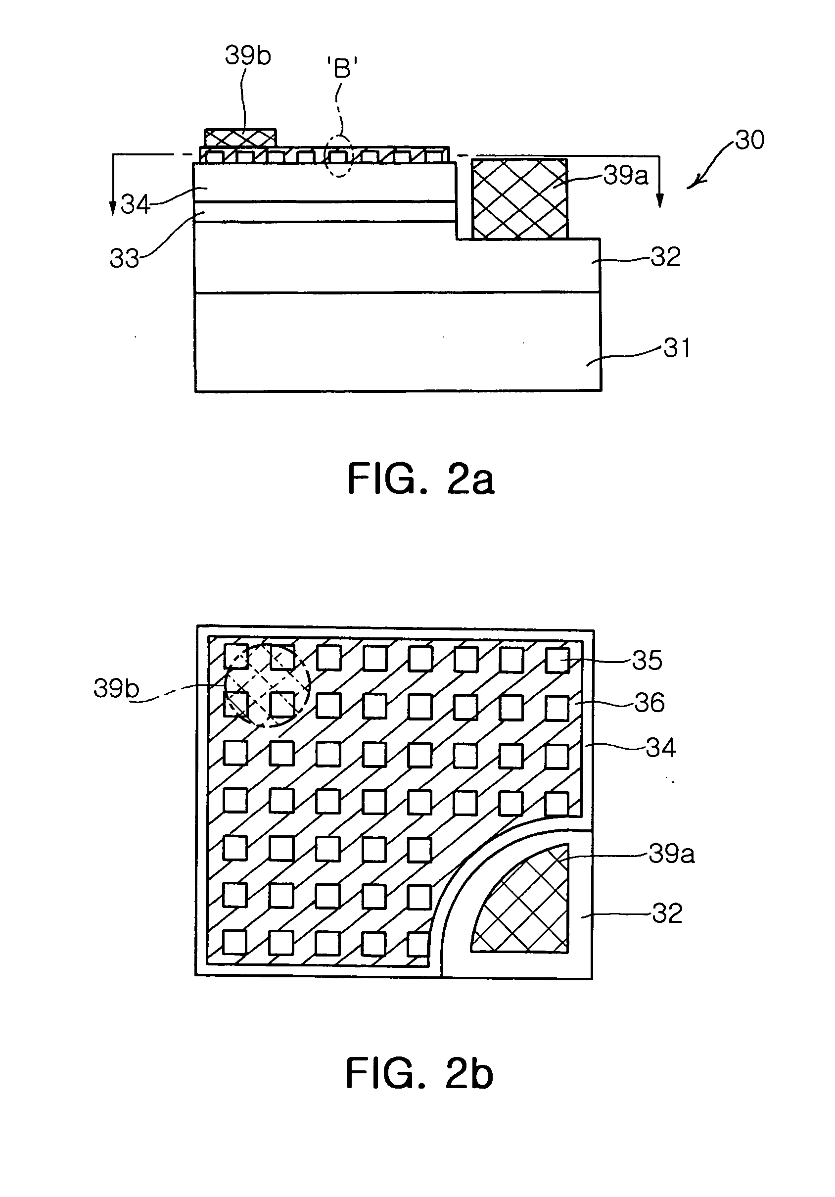
[0031] Preferred embodiments of the present invention will now be described in detail with reference to the annexed drawing. FIGS. 2a and 2b are, respectively, a cross-sectional side view and top plan view of a flip chip type nitride semiconductor light-emitting diode in accordance with one embodiment of the present invention.

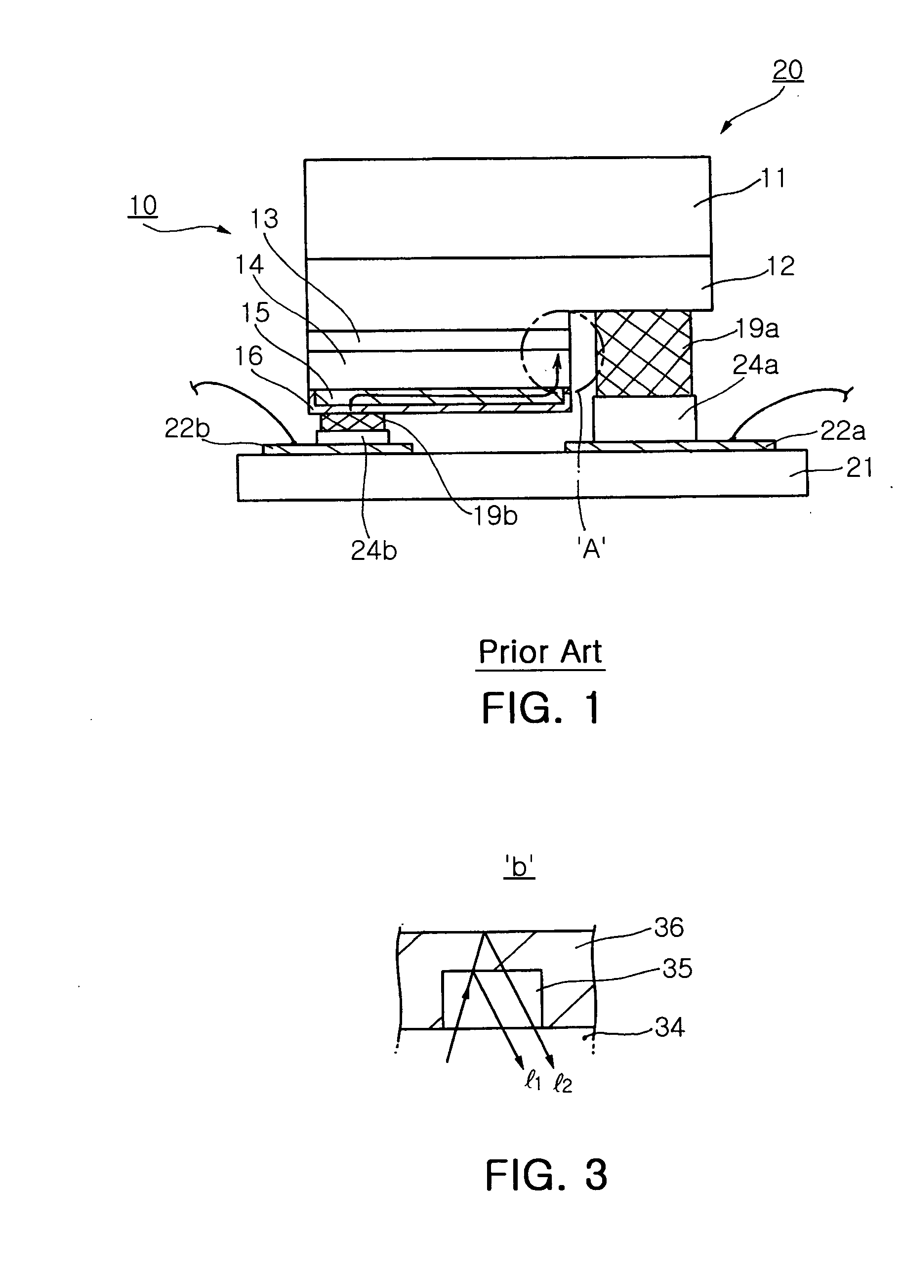
[0032] Referring to FIG. 2a, a flip chip type nitride semiconductor light-emitting diode 30 in accordance with one embodiment of the present invention comprises: a light-transmissive substrate 31 for growing nitride single crystals; an n-type nitride semiconductor layer 32 formed on the light-transmissive substrate 31; an,active layer 33 formed on the n-type nitride semiconductor layer 32; a p-type nitride semiconductor layer 34 formed on the active layer 33; a mesh-type dielectric layer 35 formed on the p-type nitride semiconductor layer 34 and having a mesh structure with a plurality of open regions in which the p-type nitride semiconductor layer 34 is expos...


PUM


Abstract

The present invention provides a flip chip type nitride semiconductor light-emitting diode comprising a light-transmissive substrate for growing nitride single crystals; an n-type nitride semiconductor layer formed on the light-transmissive substrate; an active layer formed on the n-type nitride semiconductor layer; a p-type nitride semiconductor layer formed on the active layer; a mesh-type dielectric layer formed on the p-type nitride semiconductor layer and having a mesh structure with a plurality of open regions in which the p-type nitride semiconductor layer is exposed; a highly reflective ohmic contact layer formed on the mesh-type dielectric layer and the open regions in which the p-type nitride semiconductor layer is exposed; and a p-bonding electrode and an n-electrode formed on the highly reflective ohmic contact layer and the n-type nitride semiconductor layer, respectively.

Description

BACKGROUND OF THE INVENTION [0001] 1. Field of the Invention [0002] The present invention relates to a nitride semiconductor light-emitting diode, and more particularly to a flip chip type nitride semiconductor light-emitting diode having excellent electrical properties and luminance. [0003] 2. Description of the Related Art [0004] Recently, a great deal of attention has been directed to nitride semiconductors using nitrides such as GaN, as a photoelectric material and a main core material for electronic devices, since they have excellent physical and chemical properties. In particular, a nitride semiconductor light-emitting diode produces green and blue color light and further light within the UV region, and as a result of technology advancement, has a marked improvement in luminance thereof, therefore it is also applied to full color sign boards, illumination devices, and the like. [0005] Such a nitride semiconductor light-emitting diode is a light-emitting diode to obtain light w...

Claims


Application Information

Patent Timeline
Patent Type & Authority Applications(United States)
IPC IPC(8): H01L21/00H01L33/06H01L33/10H01L33/32H01L33/36H01L33/62
CPCH01L33/32H01L33/44H01L33/405H01L33/387H01L2224/1403H01L2224/16225
Inventor KIM, DONG JOONKIM, HYUN KYUNG
Owner SAMSUNG ELECTRONICS CO LTD
Why Eureka
Try Eureka