System-in-package (SIP) structure and fabrication thereof

a technology of system-in-package and packaging, which is applied in the direction of semiconductor devices, semiconductor/solid-state device details, electrical apparatus, etc., can solve the problems of difficult thinning high cost inability to easily reduce thickness of conventional sip structures, etc., to achieve the effect of reducing thickness

Inactive Publication Date: 2005-12-08
UNITED MICROELECTRONICS CORP
View PDF9 Cites 49 Cited by
  • Summary
  • Abstract
  • Description
  • Claims
  • Application Information

AI Technical Summary

Benefits of technology

[0008] In view of the foregoing, an object of this invention is to provide a SIP structure that has a reduced thickness.

Problems solved by technology

Since the thickness of a chip is the same as that of a wafer, the thickness of the conventional SIP structures cannot be easily reduced.
Moreover, the conventional carrier substrate is usually a printed circuit board (PBC) and the bump material for wire bonding is mostly gold, so that the costs of the conventional SIP structures are higher.
Furthermore, the conventional carrier substrate, which is usually a printed circuit board (PBC), makes the conventional SIP structures difficult to thin down.

Method used


Image

  • System-in-package (SIP) structure and fabrication thereof
  • System-in-package (SIP) structure and fabrication thereof
  • System-in-package (SIP) structure and fabrication thereof

Examples


first embodiment

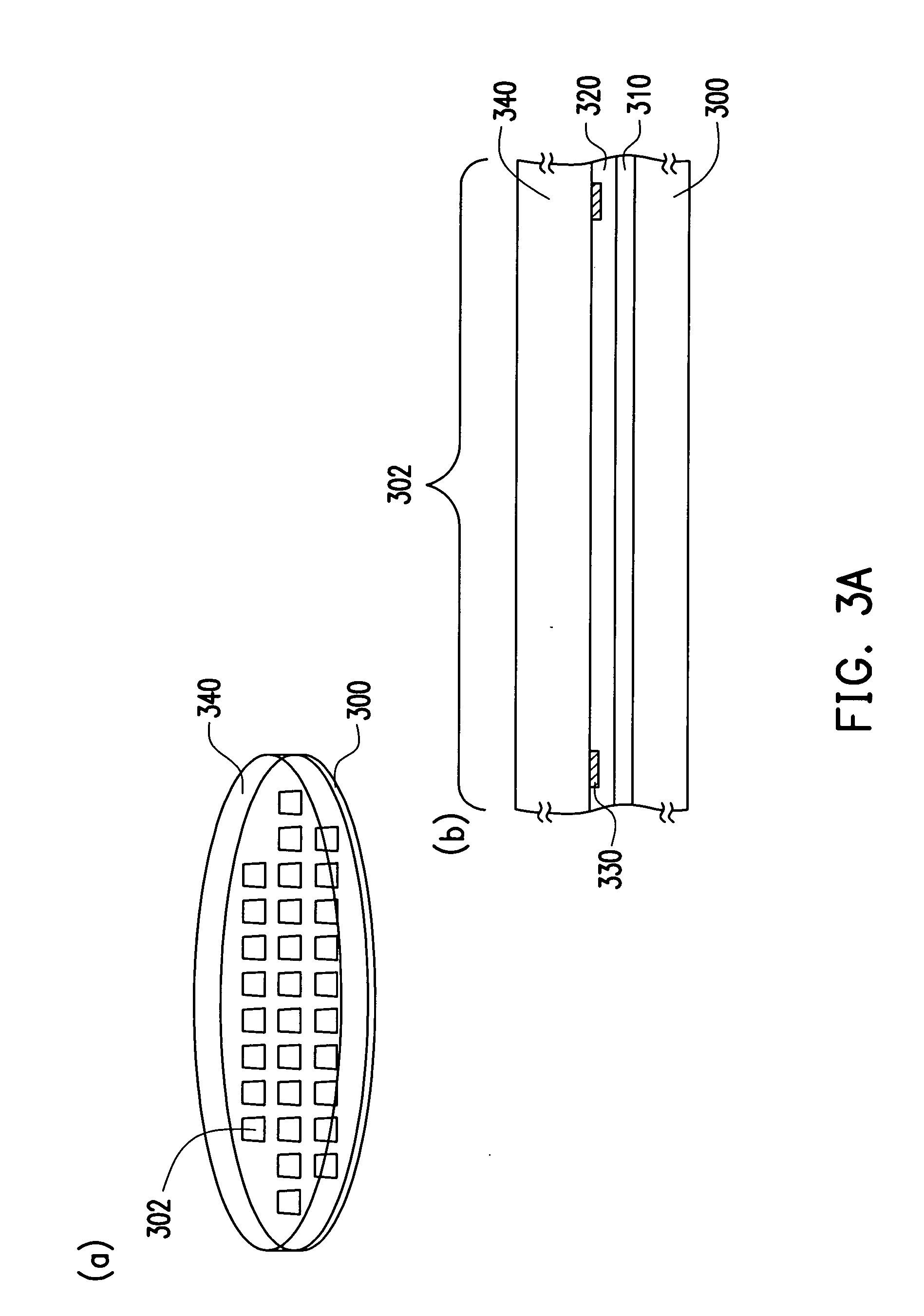
[0024] FIGS. 3A(b) and 3B-3H illustrates a process flow of fabricating an SIP structure according to the first embodiment of this invention in a local cross-sectional view, and FIG. 3A(a) illustrates the whole wafer area corresponding to FIG. 3A(b).

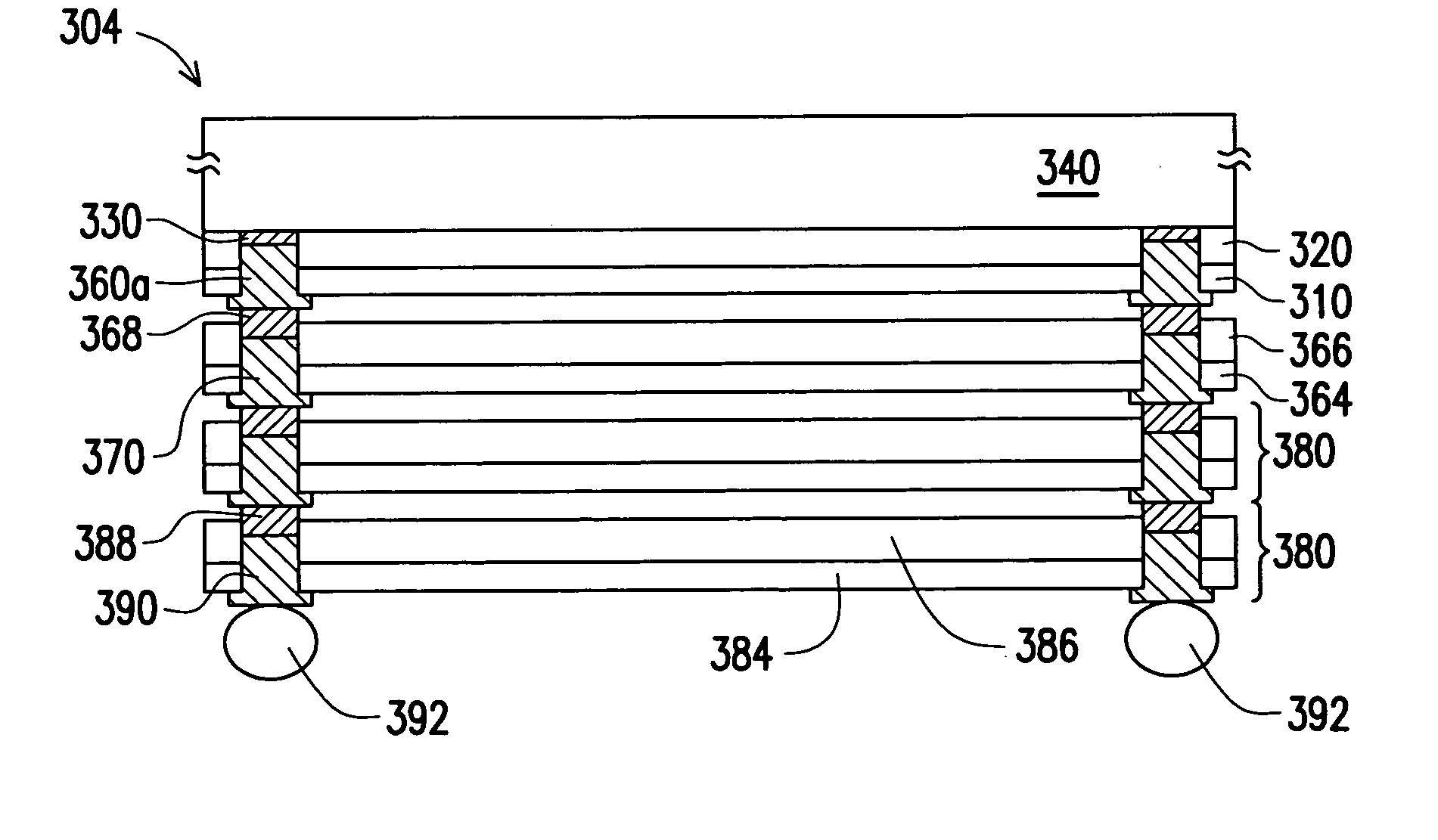
[0025] Referring to FIG. 3A(a) / (b), a semiconductor-on-insulator (SOI) wafer 300, such as, a silicon-on-insulator wafer, is provided, including an insulator 310 and a semiconductor layer thereon. The insulator 310 is a buried oxide layer, for example, and the semiconductor layer is a part of the layer 320 described latter. The thickness of the insulator 310 ranges from 1 μm to 10 μm. The SOI wafer 300 is then subjected to a complete fabricating process to form a circuit layer 320 based on the semiconductor layer and to define multiple die regions 302. The thickness of the circuit layer 320 ranges approximately from 10 μm to 100 μm, and the circuit layer 320 within each die region 302 has multiple bonding pads 330 formed thereon. Then, a ...

second embodiment

[0033]FIGS. 4A-4C illustrates a latter part of a process flow of fabricating an SIP structure according to the second embodiment of this invention in a local cross-sectional view, while the former part of the process flow may include the same steps as illustrated in FIGS. 3A-3E.

[0034] Referring to FIG. 4A, another cover plate 400 is bonded to the insulator 364 of the secondly stacked circuit / insulator composite layer 366 / 364 (FIG. 3E). The cover plate 400 can be completely the same as the cover plate 340. The material of the cover plate 400 may be glass, and the thickness of the cover plate 400 ranges approximately from 1 mm to 10 mm.

[0035] Referring to FIG. 4B, the original cover plate 340 is removed from the circuit layer 320 of the firstly stacked circuit / insulator composite layer 320 / 310 to expose the bonding pads 330 on the circuit layer 320.

[0036] Referring to FIG. 4C, after the cover plate 340 is removed, bumps 410 are formed on the bonding pads 330 of the bottom circuit l...


PUM


Abstract

A system-in-package (SIP) structure is described, including stacked circuit/insulator composite layers, bumps and a cover plate. Each circuit/insulator composite layer is lifted off from a semiconductor-on-insulator (SOI) substrate, including the insulator of the SOI substrate and a circuit layer based on the semiconductor of the SOI substrate. The circuit layer of a circuit/insulator composite layer is electrically coupled with the circuit layer of the underlying circuit/insulator composite layer. The bumps are disposed on the lower surface of the bottom circuit/insulator composite layer, electrically coupled with the circuit layer of the bottom circuit/insulator composite layer. The cover plate is disposed on the top circuit/insulator composite layer.

Description

BACKGROUND OF THE INVENTION [0001] 1. Field of the Invention [0002] The present invention relates to a semiconductor apparatus. More particularly, the present invention relates to a system-in-package (SIP) structure and a method for fabricating the same. [0003] 2. Description of the Related Art [0004] SIP technique is very useful in compactification of electronic system, and reducing the thickness of SIP is very important in related fields. In the prior art, an SIP structure is formed with wire bonding or 3D solder-ball stacking. [0005]FIG. 1 illustrates a conventional SIP structure that is usually called stacked CSP (chip-scale package). Referring to FIG. 1, the stacked CSP includes a first chip 100, a second chip 110 and a third chip 120 that are sequentially stacked on a carrier substrate 130 interposed by underfill 135. Each chip (100, 110 or 120) is electrically connected to the circuit of the carrier substrate 130 using bumps (not shown) and bonding wires 140, so that the size...

Claims


Application Information

Patent Timeline
Patent Type & Authority Applications(United States)
IPC IPC(8): H01L21/48H01L21/58H01L21/68H01L21/98H01L23/48H01L23/498H01L25/065
CPCH01L21/4857H01L2224/0401H01L23/49816H01L23/49822H01L24/05H01L24/94H01L25/0657H01L25/50H01L2221/68345H01L2221/68359H01L2224/05009H01L2224/0557H01L2224/08146H01L2224/16145H01L2224/32145H01L2224/32225H01L2224/48091H01L2224/48095H01L2224/48227H01L2224/81005H01L2225/06513H01L2225/06517H01L2225/06541H01L2225/06582H01L2924/01079H01L2924/01082H01L2924/15311H01L2924/1532H01L2924/15331H01L21/6835H01L2224/73265H01L2924/0002H01L2924/01033H01L2924/01006H01L2924/01005H01L24/48H01L2924/00014H01L2924/00H01L2224/05552H01L24/45H01L2224/45144
Inventor HSUAN, MIN-CHIH
Owner UNITED MICROELECTRONICS CORP
Why Eureka
Try Eureka