Image pickup apparatus

a pickup apparatus and image technology, applied in the field can solve the problems of reducing the efficiency of image pickup apparatus, and increasing the chip size, so as to reduce the lag of time

Inactive Publication Date: 2005-12-08
CANON KK
View PDF13 Cites 30 Cited by
  • Summary
  • Abstract
  • Description
  • Claims
  • Application Information

AI Technical Summary

Benefits of technology

[0017] The present invention has been devised in view of the above-mentioned drawbacks, and it is an object of the present invention to reduce a lag of time for accumulating photocharges among image pickup areas.
[0018] In addition, it is another object of the present invention to obtain an image with less shading.

Problems solved by technology

Therefore, there is a limitation in making the image pickup apparatus thinner, such as a digital camera upon manufacturing the apparatus using such solid-state image pickup elements.
However, since image pickup areas are arranged one-dimensionally in one direction in the above-described conventional solid-state image pickup element, a chip size increases in one direction and a problem arises in making the image pickup element compact.
As a result, a level of a read out signal may vary to cause shading or color drift in an image that is finally obtained.

Method used


Image

  • Image pickup apparatus
  • Image pickup apparatus
  • Image pickup apparatus

Examples


first embodiment

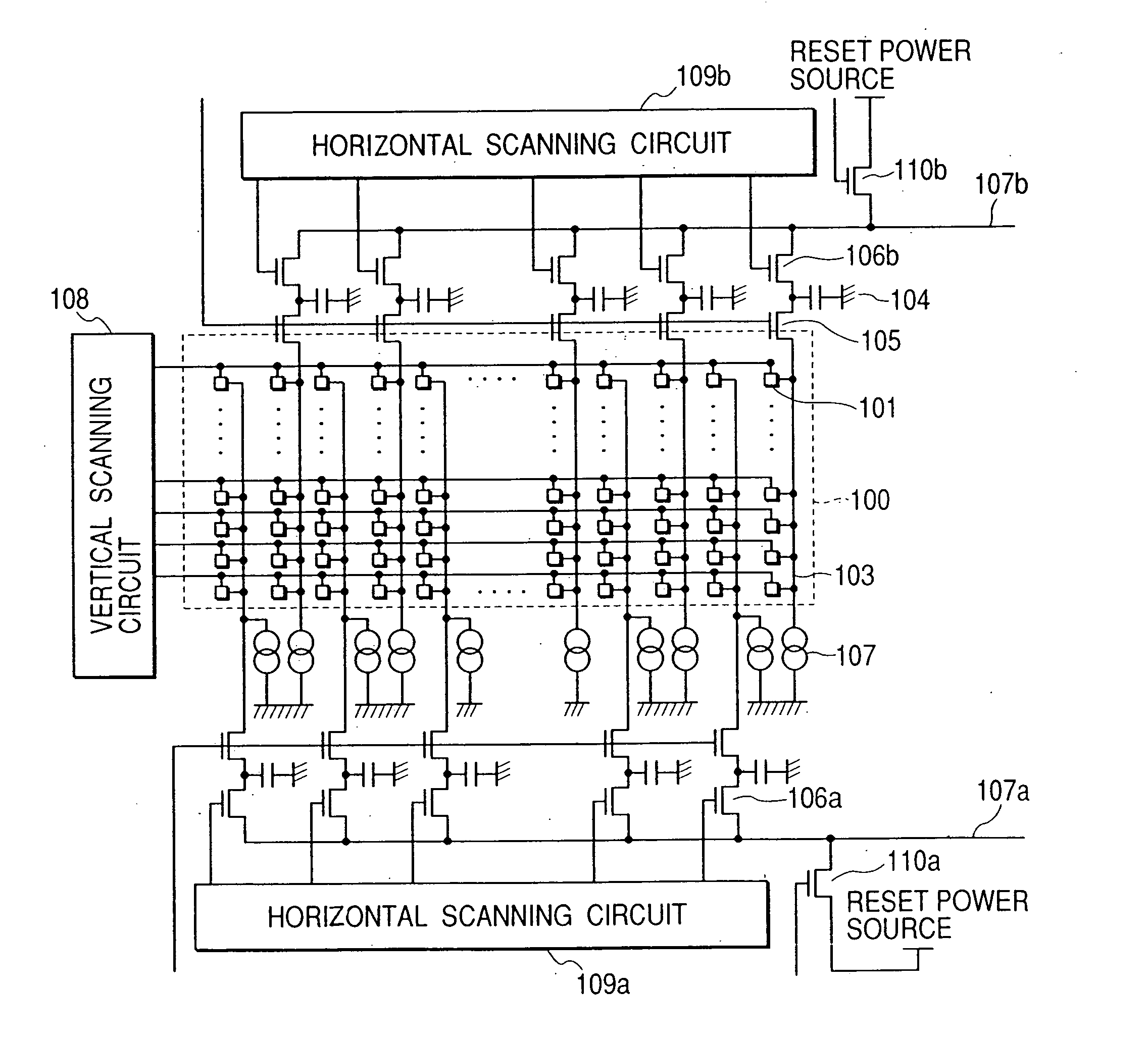
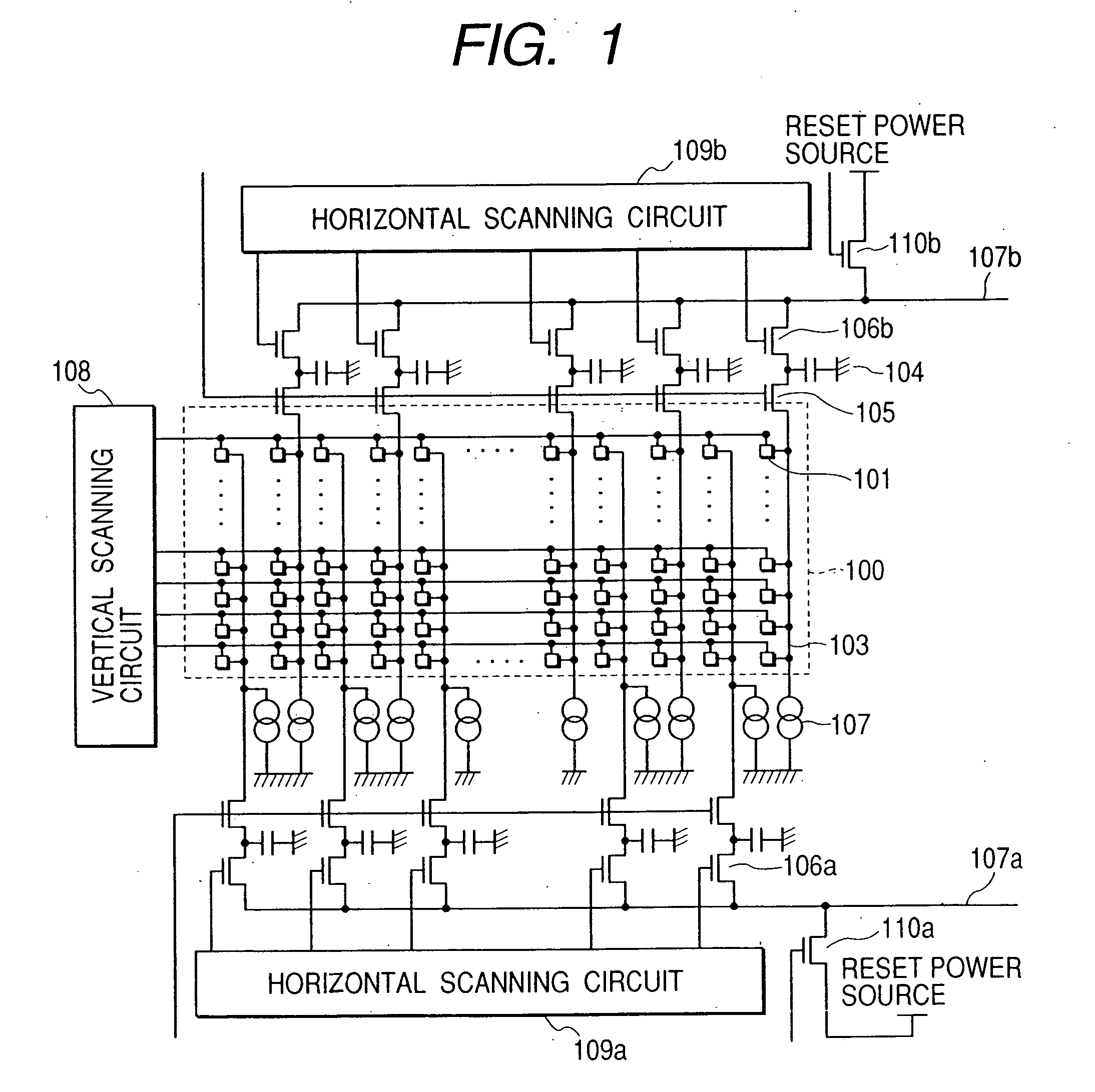
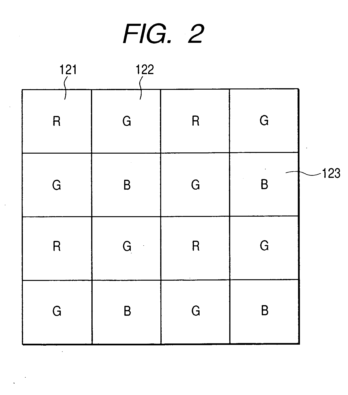
[0053]FIG. 4 is a schematic view showing a configuration of a solid-state image pickup element of the present invention, components of which are formed on a same semiconductor chip by, for example, a CMOS process. In FIG. 4, reference numeral 905 denotes pixels having a photo diode, 901 to 904 denote image pickup areas in which the pixels 905 are arranged two-dimensionally and R, G1, G2 and B filters for forming an image, respectively, are provided, 906a denotes a vertical shift register for outputting a control signal which is generated for controlling pixel scanning in the vertical direction in the image pickup areas 901 and 902, in accordance with a clock signal VCLK2 that is inputted from the outside, 906b denotes a vertical shift register that is signal supplying means for outputting a control signal which is generated for controlling pixel scanning in the vertical direction in the image pickup areas 903 and 904, in accordance with a clock signal VCLK1 that is inputted from the...

second embodiment

[0074]FIG. 6 is a schematic view showing a configuration of a solid-state image pickup element of the present invention, components of which are formed in a same semiconductor chip by the CMOS process or the like. In FIG. 6, reference symbols 910a and 911b denote line memories for accumulating charges or the like read out from the pixels 905 arranged in the R image pickup area 901 and the G1 image pickup area 902, respectively, and 911c to 911f denote horizontal shift registers for sequentially outputting charges or the like read out from the R image pickup area 901, the G1 image pickup area 902, the G2 image pickup area 903 and the B image pickup area 904 among the charges or the like retained in the line memories 910a and 911b to an external processing circuit. Further, in FIG. 6, parts similar to those shown in FIG. 4 are given identical reference numerals.

[0075] In addition, operations of the solid-state image pickup element shown in FIG. 6 are similar to those shown in FIG. 4. ...

third embodiment

[0082]FIG. 7 is a schematic view showing a configuration of a solid-state image pickup element of the present invention. In FIG. 7, reference numeral 905 denotes pixels having photoelectric conversion element, and 901 to 904 denote image pickup areas of R, G1, G2 and B in which the pixels 905 are arranged two-dimensionally to form an image, respectively, the four image pickup areas being configured to be arranged two-dimensionally. Reference symbols 906a to 906d denote vertical shift registers for controlling timing for supplying a control signal for reading out an amplified signal that is based on a charge from each pixel 905 arranged in each of the image pickup areas 901 to 904, respectively, 909 denotes horizontal signal lines for supplying a control signal to each pixel 905, 912 denotes vertical signal lines for transmitting an amplified signal read out from each pixel 905, and 911a to 911d denote horizontal shift registers for sequentially controlling the transfer of amplified ...


PUM


Abstract

An image pickup apparatus is provided, which comprises a plurality of image pickup areas formed on a same semiconductor chip and arranged in the horizontal and the vertical directions, each image pickup area having a plurality of pixels arranged in the horizontal and the vertical directions, a plurality of vertical scanning circuits which sequentially scan pixels in the vertical direction to scan a plurality of image pickup areas in the vertical direction independently from each other, a plurality of lenses, at least one of which is provided in each of the plurality of image pickup areas and which focuses light to form an image on the image pickup areas, and a driving circuit which drives the plurality of vertical scanning circuits so that at least a part of a scanning period of each of the plurality of vertical scanning circuits overlaps with each other.

Description

BACKGROUND OF THE INVENTION [0001] 1. Field of the Invention [0002] The present invention relates to an image pickup apparatus for picking up an image of a subject. [0003] 2. Related Background Art [0004] An example of a configuration of a conventional solid-state image pickup element is shown in FIG. 1. In the figure, reference numeral 101 denotes pixels having a photoelectric conversion portion such as a photo diode. A pixel area 100 on which an image of a subject is picked up is formed by arranging these pixels two-dimensionally. [0005] In addition, reference numeral 103 denotes vertical signal lines to which signals from the pixels 101 are read out, 104 denotes storage capacitors for temporarily accumulating signals read out to the vertical signal lines 103 from the pixels 101, 105 denotes transfer MOS transistors for transferring the signals read out to the vertical signal lines 103 to the storage capacitors 104, and 106a and 106b denote transfer MOS transistors for transferrin...

Claims


Application Information

Patent Timeline
Patent Type & Authority Applications(United States)
IPC IPC(8): H04N3/15H04N5/335H04N9/04
CPCH01L27/14603H01L27/14621H01L27/14625H04N2209/048H04N3/1593H04N9/045H01L27/14645H04N25/41H04N25/70H04N23/84H04N25/62H04N25/74H04N23/10
Inventor YONEDA, TOMOYAINOUE, SHUNSUKEKOCHI, TETSUNOBUTAKAHASHI, HIDEKAZUOGURA, MASANORI
Owner CANON KK
Why Eureka
Try Eureka