

Image pickup device, and image pickup device assembling method
a pickup device and image technology, applied in the field of image pickup devices, can solve the problems of limited camera size and inability to use machines, and achieve the effects of preventing distortion of pictures or degrading picture quality, convenient assembly, and efficient manufacturing
- Summary
- Abstract
- Description
- Claims
- Application Information
AI Technical Summary
Benefits of technology
Problems solved by technology
Method used
Image

Examples
embodiment 1
(Embodiment 1)
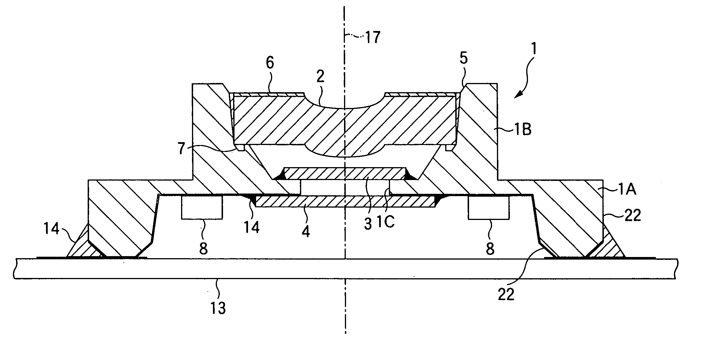
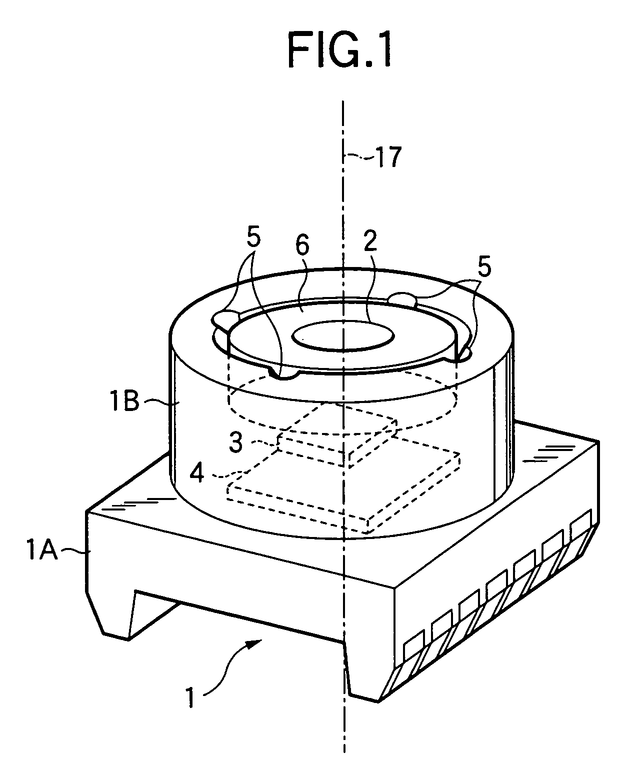
[0038]FIG. 1 is a perspective view showing the first embodiment of imaging apparatus according to the invention. FIG. 2 is a sectional view thereof. In FIGS. 1 and 2, a three-dimensional circuit board 1 is composed of a leg 1A having rectangular frustum shape and a barrel 1B thereon having the shape of a bottomed cylinder, and an opening 1C is formed at the boundary between the leg 1A and the barrel 1B and a wiring pattern 22 is formed on the back side of the leg 1A. Onto the inner circumference of the barrel 1B of the three-dimensional circuit board 1 is fit a lens 2, about whose optical axis 17 is arranged an optical filter 3 above the opening 1C, below which are arranged a semiconductor imaging device 4 and on-chip components 8. All of these components are completed when attached to a three-dimensional circuit board 1. Beneath the three-dimensional circuit board is arranged a printed circuit board 13 as a main circuit board of a portable telephone set, a PC or vario...
embodiment 2
(Embodiment 2)
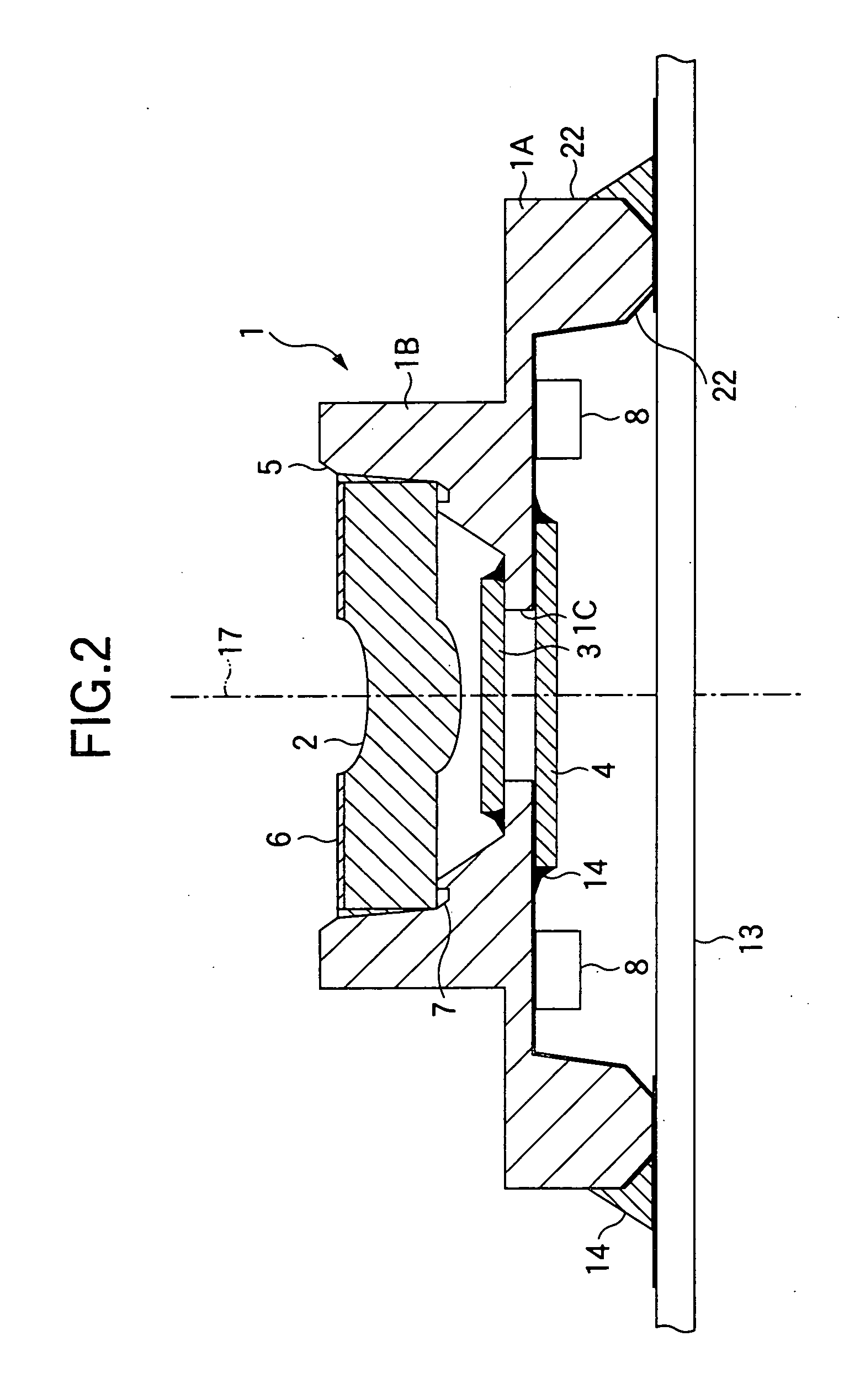
[0041]FIG. 3 is a sectional view of imaging apparatus in Embodiment 2 of the invention. For simplicity, similar members to those in Embodiment 1 are assigned the similar signs. In FIG. 3, a three-dimensional printed circuit board 1 is composed of a leg 1A having a rectangular frustum shape and a barrel 1B thereon having the shape of a bottomed cylinder, and an opening 1C is formed at the boundary between the leg 1A and the barrel 1B and a recessed shoulder 1D is formed inside the leg 1A. On the back-side of the leg 1A including the recessed shoulder 1D is formed a wiring pattern 22. Onto the inner circumference of the barrel 1B of the three-dimensional circuit board 1 is fit a lens 2, about whose optical axis 17 is arranged an optical filter above the opening 1C, below which are arranged a semiconductor imaging device 4 and on-chip components 8. On the recessed shoulder 1D beneath is arranged a printed circuit board 10 mounting an LSI 11a and on-chip components 11b on ...
PUM
 Abstract
Description
Claims
Application Information