

Apparatus and method for manufacturing tilted microlenses
a microlens and tilting technology, applied in the field of microlens array structure and manufacturing methods, can solve the problems of increasing the crosstalk between adjacent pixels, small charge accumulation area in individual pixels in the array, and increasing the difficulty of providing a microlens capable of focusing incident light rays onto the photosensitive regions, so as to achieve the effect of convenient manufacturing
- Summary
- Abstract
- Description
- Claims
- Application Information
AI Technical Summary
Benefits of technology
Problems solved by technology
Method used
Image

Examples
Embodiment Construction
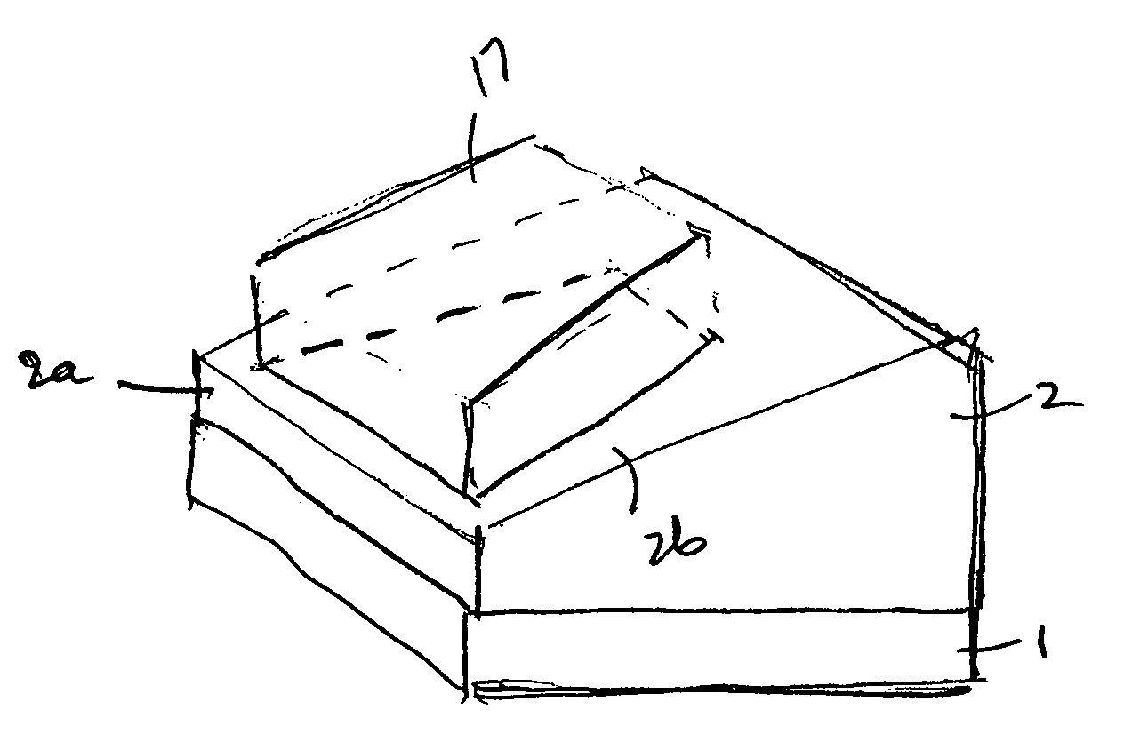
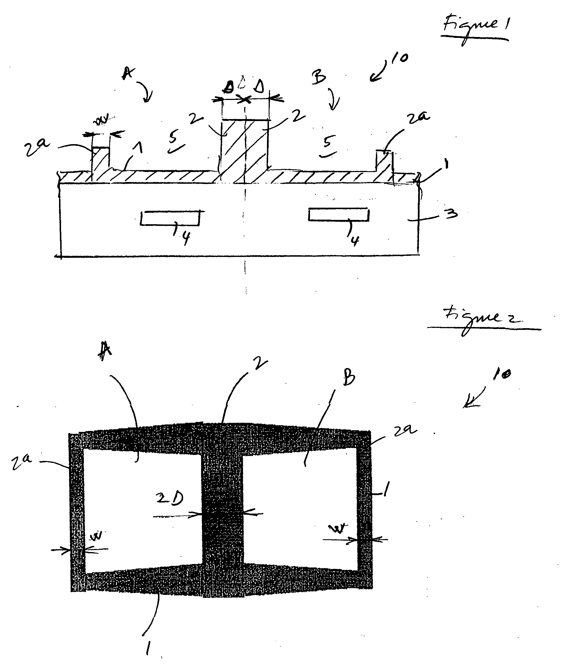
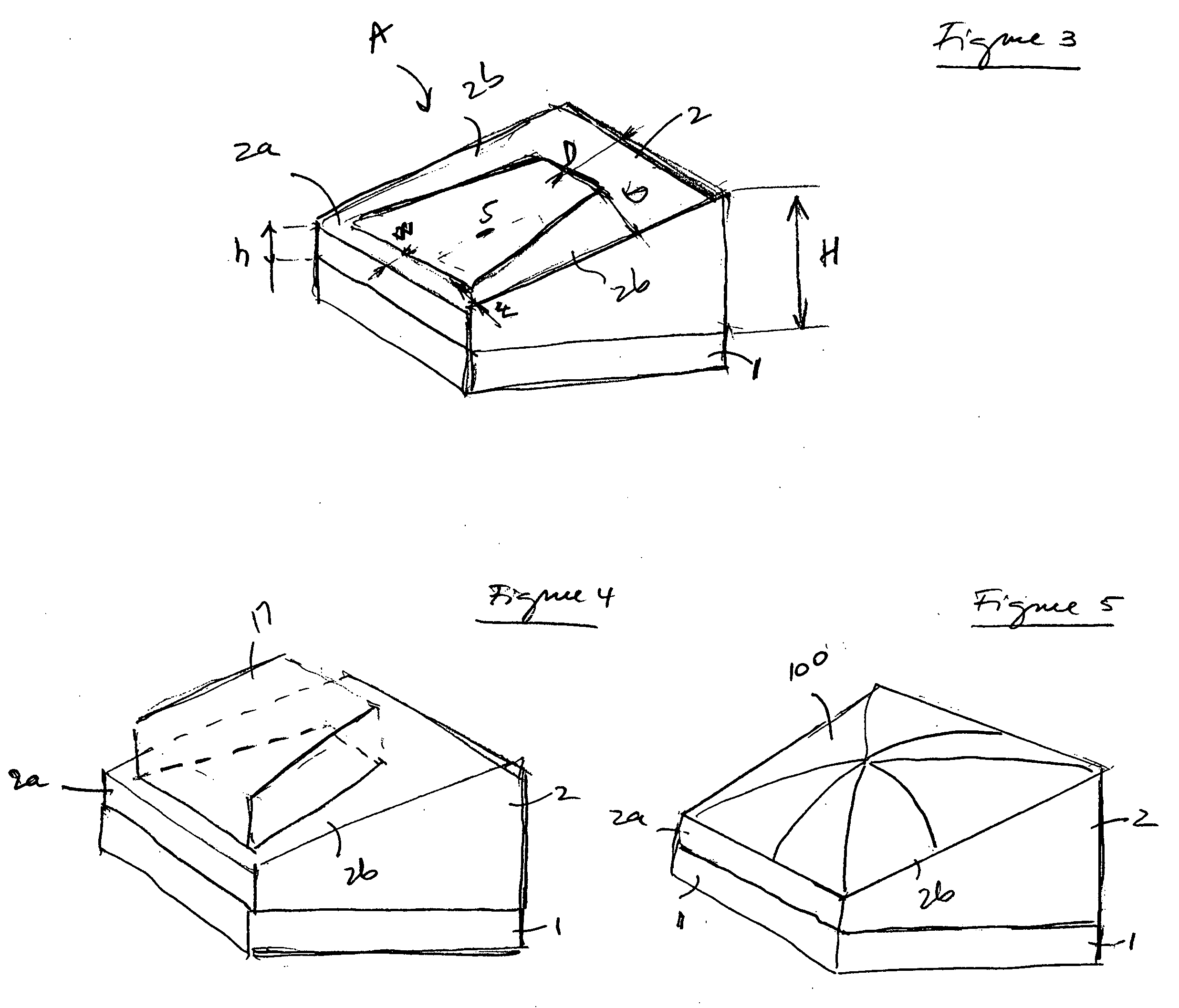
[0025] According to the invention, the focal characteristics of a microlens and its orientation can be adjusted by forming boundary walls around lens materials to contain and / or limit the outward flow of lens material. This adjusts microlens flow behavior by, for example, increasing the height of the microlens or defining a perimeter of the microlens structures. Boundary walls can be formed by forming cavities or frame sidewalls with microlens material deposited therein. Post-flow microlens orientation can also be adjusted or affected by use of asymmetrical structures formed within the microlens materials (for example, a microlens base within a microlens material) that change flow behavior of the microlens during microlens flow processing (e.g., altering the orientation of the microlens from a planar layer or a microlens cavity). In this manners asymmetrical microlenses can be formed with asymmetrical structures to provide focal points that are not directly underneath a microlens as...
PUM
 Abstract
Description
Claims
Application Information