Microprocessor with integrated high speed memory

a high-speed memory and microprocessor technology, applied in the field of micro-computer design and architecture, can solve the problems of not being able to generate two memory access addresses simultaneously in a single memory access unit, limiting the relationship between the addresses, and clearly restricting the system, so as to reduce the complexity of byte level half word, manage data transactions, and increase the bandwidth between the processor and the data cache

Inactive Publication Date: 2005-12-08
AVAGO TECH INT SALES PTE LTD
View PDF30 Cites 11 Cited by
  • Summary
  • Abstract
  • Description
  • Claims
  • Application Information

AI Technical Summary

Benefits of technology

[0012] By including read buffers or write buffers inside the load/store unit according to the present invention, the processors are directly interfaced from their load/store units to the caches. Thus, the present invention provides a computer system which is able to manage the data transactions between the processor and its cache memory substantially faster than known devices and methods for managing the interaction between processors and their data cache. A processor architecture according to the present invention deals with the two transactions per cycle from two load/store units of dual ported processor designs without making the data cache any more complicated.
[0013] Furthermore, a processor architecture according to the present invention reduces the complexity of byte level half word, full word or long word addressab

Problems solved by technology

However, these systems are clearly restricted in that, if two addresses are generated, the second address necessarily bears a certain predetermined relationship to the first address.
Vector stride units also exist which allow more than one memory address to be computed, but these are also limited in the relationship between the addresses.
Moreover, it is necessary to generate the first address prior to calcu

Method used


Image

  • Microprocessor with integrated high speed memory
  • Microprocessor with integrated high speed memory
  • Microprocessor with integrated high speed memory

Examples


Embodiment Construction

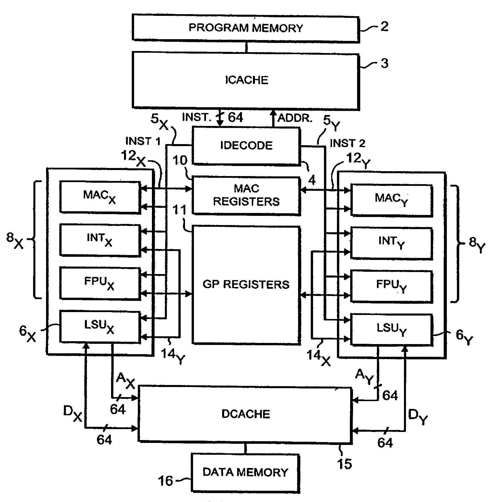
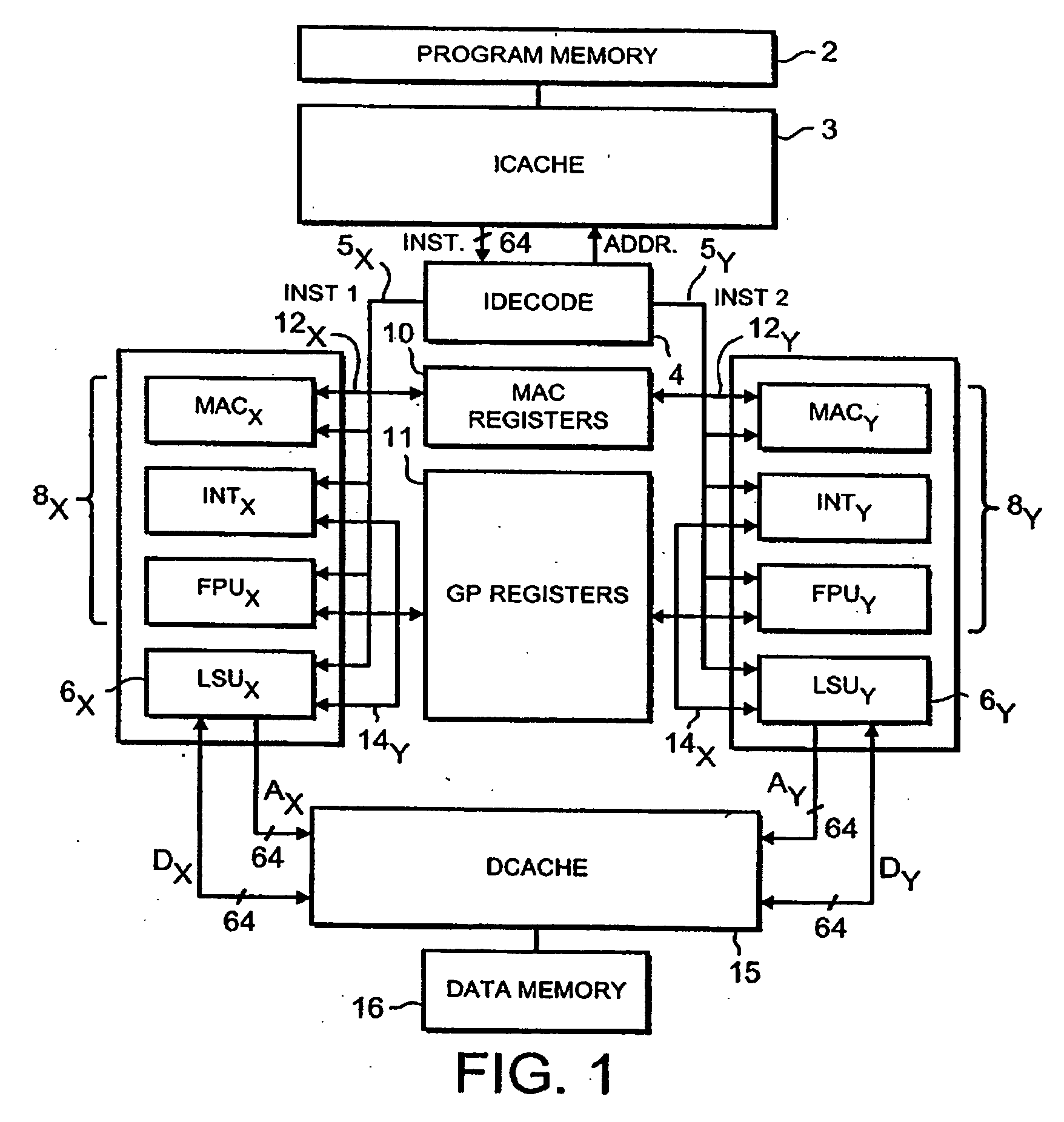
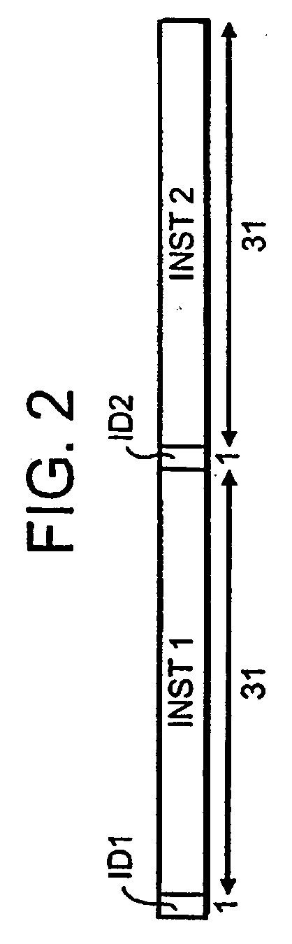
[0016] Before describing a particular implementation of the present invention, first the principle function of a known register access system will be discussed. The preferred computer system described herein is a dual instruction stream, multiple data (DIMD) stream machine which normally executes two “instructions” every cycle. FIG. 1 is a schematic diagram of a system capable of performing the present invention. In FIG. 1, reference numeral 2 denotes a program memory which holds programs in the form of a plurality of instructions. In the normal mode of operation, each 64 bit instruction in the program memory allows two 31 bit operations to be defined in the manner illustrated in FIG. 2. That is, each 64 bit instruction contains two 31 bit instruction portions labelled INST1 and INST2. Each instruction portion has associated with it a single bit which identifies the type of instruction. These are denoted ID1 and ID2 in FIG. 2, standing for identification bits. An instruction portion...


PUM


Abstract

The present invention relates to the field of (micro)computer design and architecture, and in particular to microarchitecture associated with moving data values between a (micro)processor and memory components. Particularly, the present invention relates to a computer system with an processor architecture in which register addresses are generated with more than one execution channel controlled by one central processing unit with at least one load/store unit for loading and storing data objects, and at least one cache memory associated to the processor holding data objects accessed by the processor, wherein said processor's load/store unit contains a high speed memory directly interfacing said load/store unit to the cache. The present invention improves the of architectures with dual ported microprocessor implementations comprising two execution pipelines capable of two load/store data transactions per cycle. By including a cache memory inside the load/store unit, the processor is directly interfaced from its load/store units to the caches. Thus, the present invention accelerates data accesses and transactions from and to the load/store units of the processor and the data cache memory.

Description

FIELD OF THE INVENTION [0001] The present invention relates to the field of (micro)computer design and architecture, and in particular to microarchitecture associated with moving data values between a (micro)processor and memory components. Particularly, the present invention relates to a computer system and to a method for operating said computer system with an processor architecture in which register addresses are generated with more than one execution channel controlled by one central processing unit. BACKGROUND OF THE INVENTION [0002] Known computer designs have a direct connection between the processor and its memory components. In conventional designs data values are exchanged between the processor and the memory components containing load / store addresses and load / store data objects going in and out of the processor. In more sophisticated designs additional to the data values instruction addresses and instruction data objects are going out of the output side of the processor. ...

Claims


Application Information

Patent Timeline
IPC IPC(8): G06F9/345G06F9/38G06F9/40
CPCG06F9/30036G06F9/3455G06F9/30043
Inventor WILSON, SOPHIEREDFORD, JOHN E.
Owner AVAGO TECH INT SALES PTE LTD
Why Eureka
Try Eureka