Multi-layer gate stack structure comprising a metal layer for a fet device, and method for fabricating the same

a technology of digital magnetic memory cell and metal layer, which is applied in the direction of electrical apparatus, semiconductor devices, radio frequency controlled devices, etc., can solve the problems of unsuitable gate dielectric to resist a longer overetching, unfavorable increase in wordline resistance, and high gate stack structure, etc., to achieve the effect of lowering the final gate stack structure heigh

a technology of digital magnetic memory cell and metal layer, which is applied in the direction of electrical apparatus, semiconductor devices, radio frequency controlled devices, etc., can solve the problems of unsuitable gate dielectric to resist a longer overetching, unfavorable increase in wordline resistance, and high gate stack structure, etc., to achieve the effect of lowering the final gate stack structure heigh

US20050275046A1Inactive Publication Date: 2005-12-15NAN YA TECH +1

Image

  • Multi-layer gate stack structure comprising a metal layer for a fet device, and method for fabricating the same
  • Multi-layer gate stack structure comprising a metal layer for a fet device, and method for fabricating the same
  • Multi-layer gate stack structure comprising a metal layer for a fet device, and method for fabricating the same

Examples


Embodiment Construction

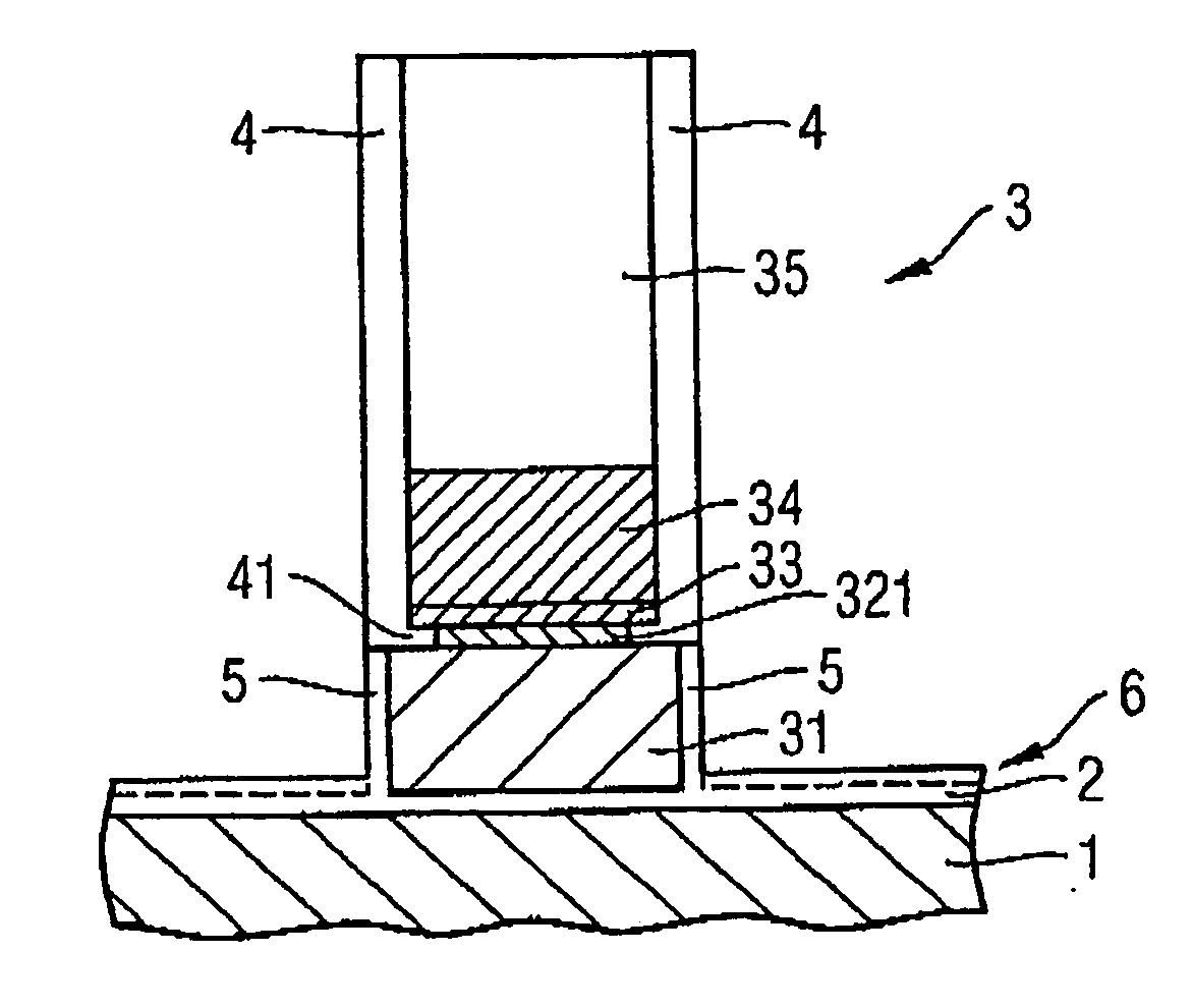
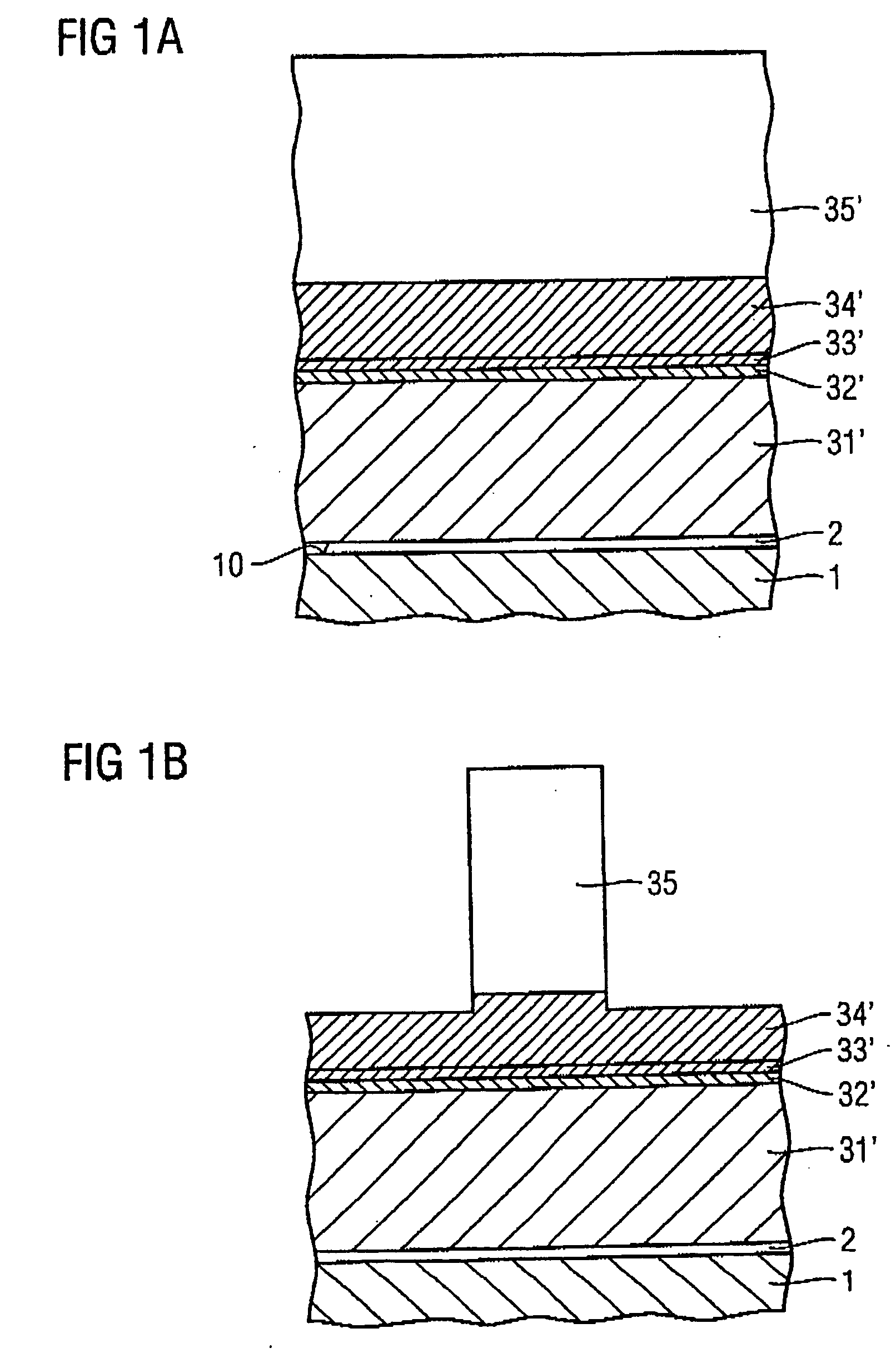
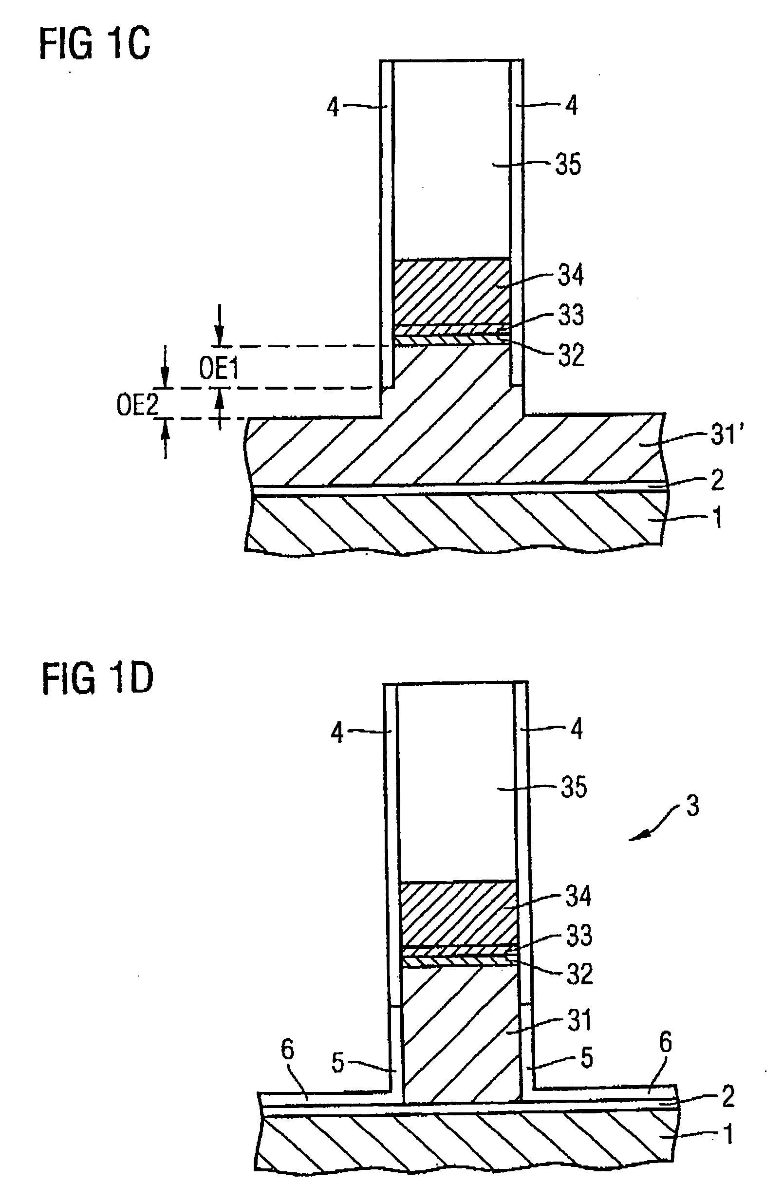
[0026] In the figures, the same reference numbers are used to indicate the same or corresponding elements. Further, each layer is named by its reference number, amended by a prime (′) after deposition. The corresponding patterned layers are marked by the reference numbers without prime. A list of reference symbols utilized consistently in the figures is provided below:

List of Reference Symbols

[0027]1 semiconductor substrate [0028]10 substrate surface [0029]2 gate dielecric [0030]3 gate stack structure [0031]31′ deposited polysilicon layer [0032]−patterned polysilicon layer [0033]32′ deposited interface layer [0034]32 patterned interface layer [0035]320 interface layer divot [0036]321 pulled back interface layer [0037]33′ deposited barrier layer [0038]33 patterned barrier layer [0039]34′ deposited metal layer [0040]34 patterned metal layer [0041]35′ cap dielectric layer [0042]35 cap dielectric [0043]4 dielectric passivation liner [0044]41 divot fill [0045]5 dielectric sidewall line...


PUM

PropertyMeasurementUnit
widthaaaaaaaaaa
thicknessaaaaaaaaaa
thicknessaaaaaaaaaa

Abstract

A multi-layer gate stack structure of a field-effect transistor device is fabricated by providing a gate electrode layer stack with a polysilicon layer, a transition metal interface layer, a nitride barrier layer and then a metal layer on a gate dielectric, wherein the transition metal is titanium, tantalum or cobalt. Patterning the gate electrode layer stack comprises a step of patterning the metal layer and the barrier layer with an etch stop on the surface of the interface layer. Exposed portions of the interface layer are removed and the remaining portions are pulled back from the sidewalls of the gate stack structure leaving divots extending along the sidewalls of the gate stack structure between the barrier layer and the polysilicon layer. A nitride liner encapsulating the metal layer, the barrier layer and the interface layer fills the divots left by the pulled-back interface layer. The nitride liner is opened before the polysilicon layer is patterned. As the requirement for an overetch into the polysilicon layer during the etch of the metal layer, the barrier layer and the interface layer is omitted, the height of the polysilicon layer can be reduced. The aspect ration of the gate stack structure is improved, the feasibility of pattern and fill processes enhanced and the range of an angle under which implants can be performed is extended.

Description

BACKGROUND [0001] 1. Field of the Invention [0002] The following relates to a method and apparatus for homogeneously magnetizing an exchange-coupled layer system of a digital magnetic memory cell device comprising an AAF layer system and an antiferromagnetic layer that exchange-couples a layer of the AAF layer system. [0003] 2. Background Information [0004] Conventional integrated circuits comprise FET devices with an active area consisting of a source region, a drain region and a channel region between the source region and the drain region formed respectively in a semiconductor substrate beneath a substrate surface of the semiconductor substrate. Gate electrodes of the FET devices are formed above the channel region on a gate dielectric covering the substrate surface. [0005] The gate electrodes of the FET devices are provided by first depositing a sequence of layers for a gate electrode layer stack on the gate dielectric and then patterning the gate electrode layer stack. In memor...

Claims


Application Information

Patent Timeline
15 Dec 2005
Publication
US20050275046A1
IPC
H01L21/28; H01L21/3205; H01L31/062
CPC
H01L21/28044; H01L21/18; B82Y40/00
Inventors
GOLDBACH, MATTHIAS; JAKUBOWSKI, FRANK