Magnetic detecting element having antiferromagnetic film having predetermined space in track width direction and method for manufacturing the same

a technology of antiferromagnetic film and magnetic detecting element, which is applied in the field of magnetic detecting element, can solve the problems of increasing the significance of the decrease in the reproduction output, the current loss, and the decrease of the reproduction output, and achieve the effect of improving the reproduction outpu

Inactive Publication Date: 2005-12-15
TDK CORPARATION
View PDF10 Cites 13 Cited by
  • Summary
  • Abstract
  • Description
  • Claims
  • Application Information

AI Technical Summary

Benefits of technology

[0029] The present invention has been achieved for solving the above problems, and an object of the present invention is to provide a magnetic detecting element comprising a pinned magnetic layer and a first antiferromagnetic layer whose

Problems solved by technology

However, the structure of the magnetic detecting element shown in FIG. 63 has the following problems.
However, in the structure shown in FIG. 63, the sensing current easily shunts to the antiferromagnetic layer 1 formed below the bottom of the pinned magnetic layer 2 to cause a current loss, thereby causing the problem of decreasing reproduction output.
However, the decrease in reproduction output becomes more significant as the track width Tw decreases, and thus a shunt sensing current shunting to the antiferromagnetic layer 1 has a considerable problem.
However, the above-described current loss increases due to the large thickness of the antiferromagnetic layer 1, and the distance between shield layers 7 and 8 formed at the top and bottom of the magnetic detecting element in the thickness direction (the Z direction shown in the drawing) cannot be decreased, failing to manufacture the magnetic detecting element adaptable for a narrower gap.
Furthermore, as shown in FIG. 63, when the antiferromagnetic layer 1 is formed below the entire bottom of the pinned magnetic layer 2, a magnetic detecting element resistant to electrostatic damage (ESD) cannot be manufactured.
However, at present, the element decreases in size, and thus heat at a temperature over the blocking temperature is generated in the element, thereby causing a magnetic electros

Method used


Image

  • Magnetic detecting element having antiferromagnetic film having predetermined space in track width direction and method for manufacturing the same
  • Magnetic detecting element having antiferromagnetic film having predetermined space in track width direction and method for manufacturing the same
  • Magnetic detecting element having antiferromagnetic film having predetermined space in track width direction and method for manufacturing the same

Examples


examples

[0421] The magnetic detecting elements having the structures shown in FIGS. 50 (Example) and 53 (Comparative Example), respectively, were used for determining unidirectional exchange bias magnetic field Hex* and reproduction output (normalized output).

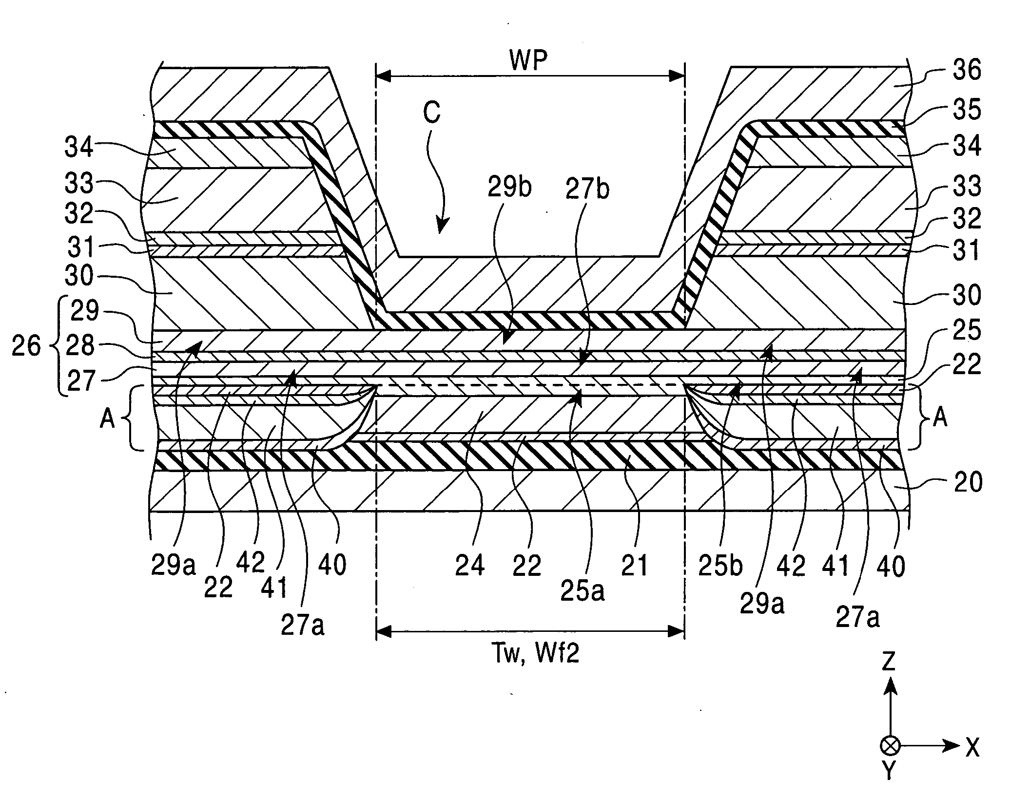
[0422]FIG. 50 (Example) is a schematic drawing showing a partial section of the magnetic detecting element, as viewed from a surface facing a recording medium. In FIG. 50, a film structure comprises a seed layer: (Ni0.8Fe0.2)60at %Cr40at % (60 Å) / a free magnetic layer: Ni80at %Fe20at % (35 Å) / CO90at %Fe10at % (10 Å) / a nonmagnetic material layer: Cu (21 Å) / a pinned magnetic layer: [second magnetic layer: CO90at %Fe10at % (X Å) / nonmagnetic intermediate layer: Ru (9 Å) / first magnetic layer: CO90at %Fe10at % (Y Å)] / a first antiferromagnetic layer: Pt50at %Mn50at % (200 Å). In this structure, a value in parentheses shows the thickness of each layer. As shown in FIG. 50, magnetization of the free magnetic layer is oriented in the track widt...


PUM


Abstract

The present invention provides a magnetic detecting element including a pinned magnetic layer and a first antiferromagnetic layer which constitutes an exchange coupling film and the structures of which are optimized for properly pinning magnetization of the pinned magnetic layer, improving reproduction output and properly complying with a narrower gap, and a method of manufacturing the magnetic detecting element. The pinned magnetic layer has a synthetic ferrimagnetic structure, and the first antiferromagnetic layer has a predetermined space C formed at the center in the track width direction to produce exchange coupling magnetic fields only between the first antiferromagnetic layer and both side portions of a first magnetic layer of the pinned magnetic layer. Therefore, the magnetization of the pinned magnetic layer can be pinned, and an improvement in reproduction output and gap narrowing can be realized. Furthermore, a magnetic detecting element with high resistance to electrostatic damage (ESD) can be manufactured. Thus, a magnetic detecting element adaptable for a future higher recording density can be provided.

Description

BACKGROUND OF THE INVENTION [0001] 1. Field of the Invention [0002] The present invention relates to a magnetic detecting element such as a spin valve thin film element mounted on a hard disk device or the like. Particularly, the present invention relates to a magnetic detecting element comprising a pinned magnetic layer and first antiferromagnetic layer whose structures are optimized for properly pinning magnetization of the pinned magnetic layer, improving reproduction output, and properly complying with a narrower gap, and a method for manufacturing the magnetic detecting element. [0003] 2. Description of the Related Art [0004]FIG. 63 is a partial sectional view of a conventional magnetic detecting element (spin valve thin film element), as viewed from a surface facing a recording medium. [0005] In FIG. 63, reference numeral 1 denotes an antiferromagnetic layer made of PtMn or the like, a pinned magnetic layer 2 made of a NiFe alloy, a nonmagnetic material layer 3 made of Cu, and...

Claims


Application Information

Patent Timeline
IPC IPC(8): G11B5/39G01R33/09H01F10/16H01F10/32H01L43/08H01L43/10H01L43/12
CPCB82Y25/00G01R33/093Y10T428/115Y10T428/1129Y10T428/1193Y10T428/1171Y10T428/1157Y10T428/1143
Inventor HASEGAWA, NAOYAUMETSU, EIJISAITO, MASAMICHIIDE, YOSUKE
Owner TDK CORPARATION
Why Eureka
Try Eureka