Nanotube-based transfer devices and related circuits

a transfer device and nanotube technology, applied in nanoinformatics, relays, instruments, etc., can solve the problems of low density, low capacitance, and limited density of bipolar digital integrated circuits, and achieve the effect of increasing problems such as leakage current, no forward voltage drop, and low capacitan

Inactive Publication Date: 2005-12-22
NANTERO
View PDF82 Cites 65 Cited by
  • Summary
  • Abstract
  • Description
  • Claims
  • Application Information

AI Technical Summary

Problems solved by technology

However, the density of bipolar digital integrated circuits is limited by their high power consumption and the ability of packaging technology to dissipate the heat produced while the circuits are operating.
The density and operating speed of MOS digital circuits are still limited by the need to dissipate the heat produced when the device is operating.
Digital logic integrated circuits constructed from bipolar or MOS devices do not function correctly under conditions of high heat or extreme environments.
As leakage current increases, the operating temperature of the device rises, the power consumed by the circuit increases, and the difficulty of discriminating the off state from the on state reduces circuit reliability.
Conventional digital logic circuits also short internally when subjected to certain extreme environments because electrical currents are generated inside the semiconductor material.
It is possible to manufacture integrated circuits with special devices and isolation techniques so that they remain operational when exposed to such environments, but the high cost of these devices limits their availability and practicality.
In addition, such digital circuits exhibit timing differences from their normal counterparts, requiring additional design verification to add protection to an existing design.
Integrated circuits constructed from either bipolar or FET switching elements are volatile.
Alternative solutions to avoid losing information in volatile digital circuits, such as battery backup, also add cost and complexity to digital designs.
ROM is relatively low cost but cannot be rewritten.
EEPROM (or “Flash”) is inexpensive, and has low power consumption but has long write cycles (ms) and low relative speed in comparison to DRAM or SRAM.
Flash also has a finite number of read / write cycles leading to low long-term reliability.
SRAM does not need to be refreshed and is fast relative to DRAM, but has lower density and is more expensive relative to DRAM.
Both SRAM and DRAM are volatile, meaning that if power to the memory is interrupted, the memory will lose the information stored in the memory cells.
Consequently, existing technologies are either non-volatile but are not randomly accessible and have low density, high cost, and limited ability to allow multiples writes with high reliability of the circuit's function, or they are volatile and complicate system design or have low density.
A different memory cell based upon magnetic tunnel junctions has also been examined but has not led to large-scale commercialized MRAM devices.
FRAM suffers from a large memory cell size, and it is difficult to manufacture as a large-scale integrated component.
While the nonvolatility condition is met, this technology appears to suffer from slow operations, difficulty of manufacture and reliability and has not reached a state of commercialization.
This form of memory requires highly specialized wire junctions and may not retain non-volatility owing to the inherent instability found in redox processes.

Method used


Image

  • Nanotube-based transfer devices and related circuits
  • Nanotube-based transfer devices and related circuits
  • Nanotube-based transfer devices and related circuits

Examples


Embodiment Construction

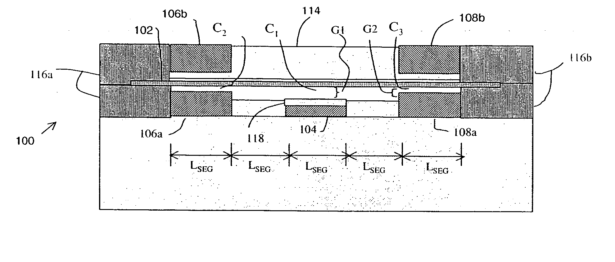
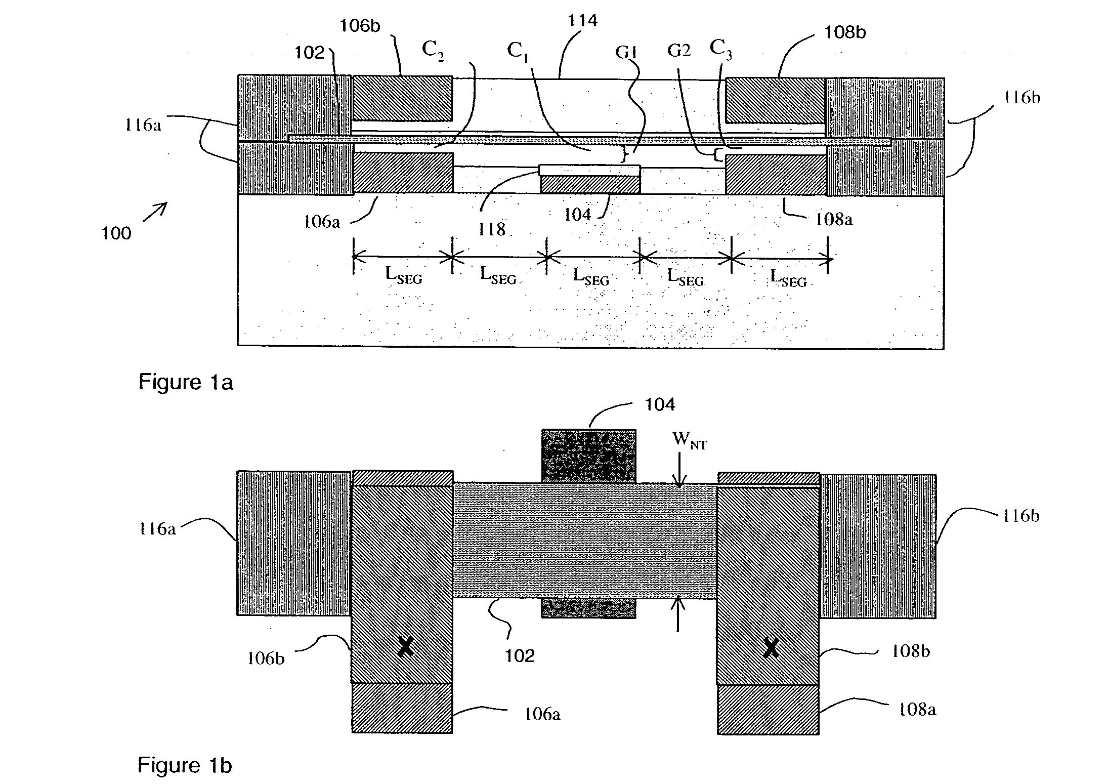
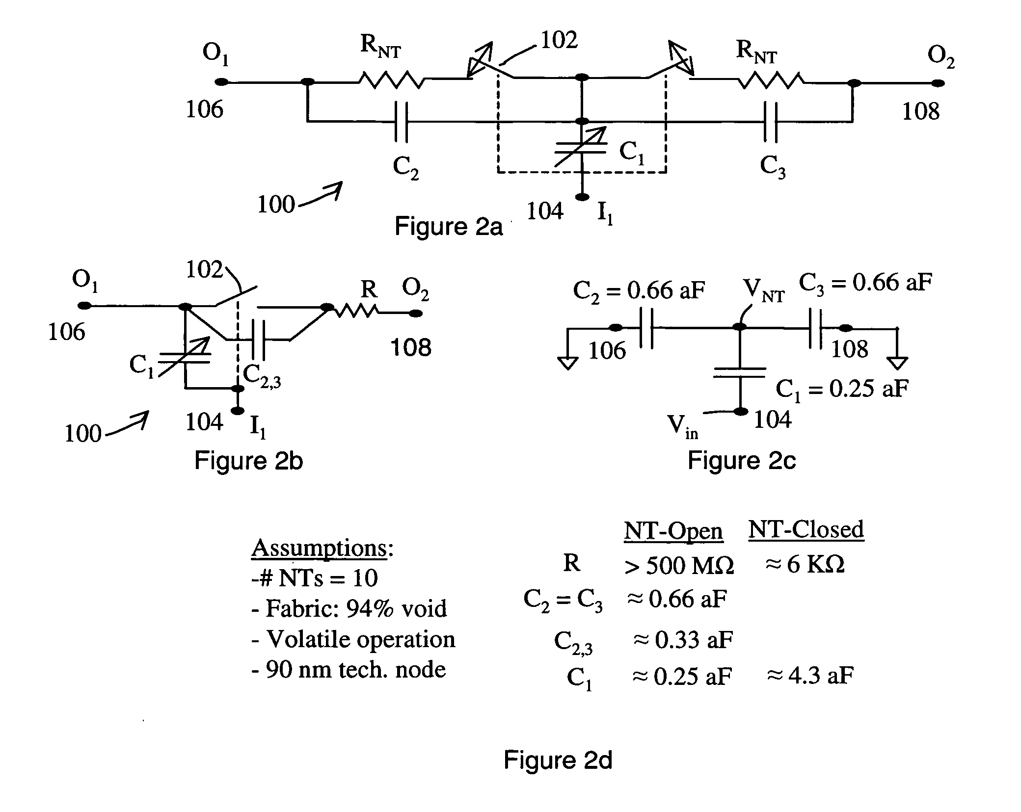
[0066] The invention provides nanotube transfer devices that controllably form a nanotube-based electrically conductive channel between a first node and a second node under the control of a control node, and also provides electrical circuits incorporating such nanotube transfer devices. The electrical potential at the control node induces a nanotube channel element to deflect into contact with or away from an electrode at each node. Each output node may be connected to an arbitrary network of electrical components. In certain embodiments, electrical circuits are designed to ensure proper switching of nanotube transfer devices interconnected with arbitrary circuits. The nanotube transfer device may be volatile or non-volatile. In preferred embodiments, the nanotube transfer device is a three-terminal device or a four-terminal device. The nanotube transfer device of various embodiments can be interconnected with other nanotube transfer devices, nanotube-based logic circuits, nanotube ...


PUM


Abstract

Nanotube transfer devices controllably form a nanotube-based electrically conductive channel between a first node and a second node under the control of a control structure. A control structure induces a nanotube channel element to deflect so as to form and unform the conductive channel between the nodes. The nanotube channel element is not in permanent electrical contact with either the first node or the second node. The nanotube channel element may have a floating potential in certain states of the device. Each output node may be connected to an arbitrary network of electrical components. The nanotube transfer device may be volatile or non-volatile. In preferred embodiments, the nanotube transfer device is a three-terminal device or a four-terminal device. Electrical circuits are provided that ensure proper switching of nanotube transfer devices interconnected with arbitrary circuits. The circuits may overdrive the control structure to induce the desired state of channel formation.

Description

CROSS-REFERENCE TO RELATED APPLICATIONS [0001] This application claims the benefit of U.S. Provisional Patent Application Ser. No. 60 / 580,799 filed Jun. 18, 2004, entitled Carbon Nanotube Microswitch Transfer Devices, the entire contents of which are incorporated herein by reference. [0002] This application is related to the following applications: [0003] U.S. patent application Ser. No. 10 / 917,794, filed on Aug. 13, 2004, entitled Nanotube-Based Switching Elements; [0004] U.S. patent application Ser. No. 10 / 918,085, filed on Aug. 13, 2004, entitled Nanotube-Based Switching Elements With Multiple Controls; [0005] U.S. patent application Ser. No. 10 / 918,181, filed on Aug. 13, 2004, entitled Nanotube Device Structure And Methods Of Fabrication; [0006] U.S. patent application Ser. No. 10 / 917,893, filed on Aug. 13, 2004, entitled Nanotube-Based Switching Elements And Logic Circuits; [0007] U.S. patent application Ser. No. 10 / 917,606, filed on Aug. 13, 2004, entitled Isolation Structure ...

Claims


Application Information

Patent Timeline
Patent Type & Authority Applications(United States)
IPC IPC(8): G11C13/02H01H59/00H01L27/14H01L27/20H01L29/06H01L51/00H01L51/05H01L51/30
CPCH01L51/0545B82Y10/00H01L51/0052H01L51/0048G11C13/025H10K85/221H10K85/615H10K10/466
Inventor BERTIN, CLAUDE L.
Owner NANTERO
Why Eureka
Try Eureka