Image sensor with optical guard ring and fabrication method thereof

Active Publication Date: 2005-12-22
TAIWAN SEMICON MFG CO LTD
View PDF17 Cites 53 Cited by
  • Summary
  • Abstract
  • Description
  • Claims
  • Application Information

AI Technical Summary

Benefits of technology

[0020] The present invention improves on the conventional technology in that the image sensor device has an optical guard ring (or metal shield) formed in the STI structure between photosensor and light emitting element. The optical guard ring prevents photons from the light emitting element from striking the photosensor. The

Problems solved by technology

The photons (or light) emission 20 can penetrate the STI structure 3 and strike the photodiode element 12, thereby causing noise and crosstalk, and seriously

Method used


Image

  • Image sensor with optical guard ring and fabrication method thereof
  • Image sensor with optical guard ring and fabrication method thereof
  • Image sensor with optical guard ring and fabrication method thereof

Examples


first embodiment

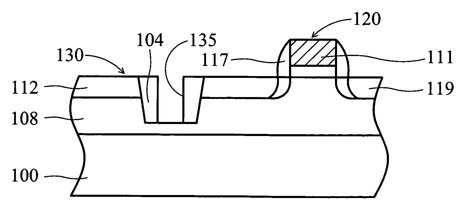
[0030]FIGS. 3A-3H are sectional views of a modified image sensor device according to an embodiment of the present invention and showing a method of manufacturing the modified image sensor device. FIG. 3H also illustrates the improved performance of the preferred embodiment of the present invention. It is noted that the first embodiment of the present invention describes the method of forming a single photodiode of a CMOS imager sensor, but is intended to be representative of all the other photodiodes on the same CMOS image sensor.

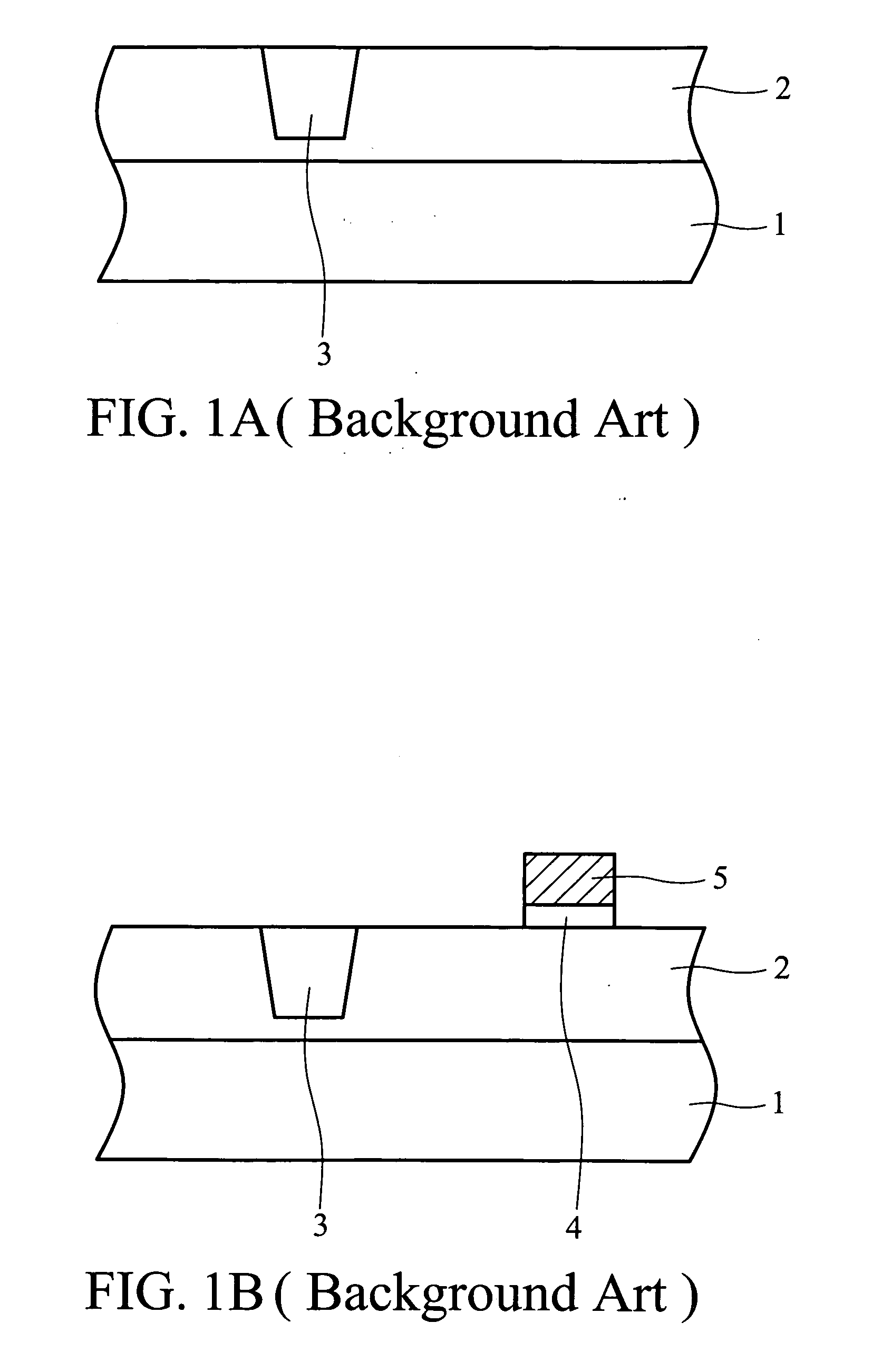
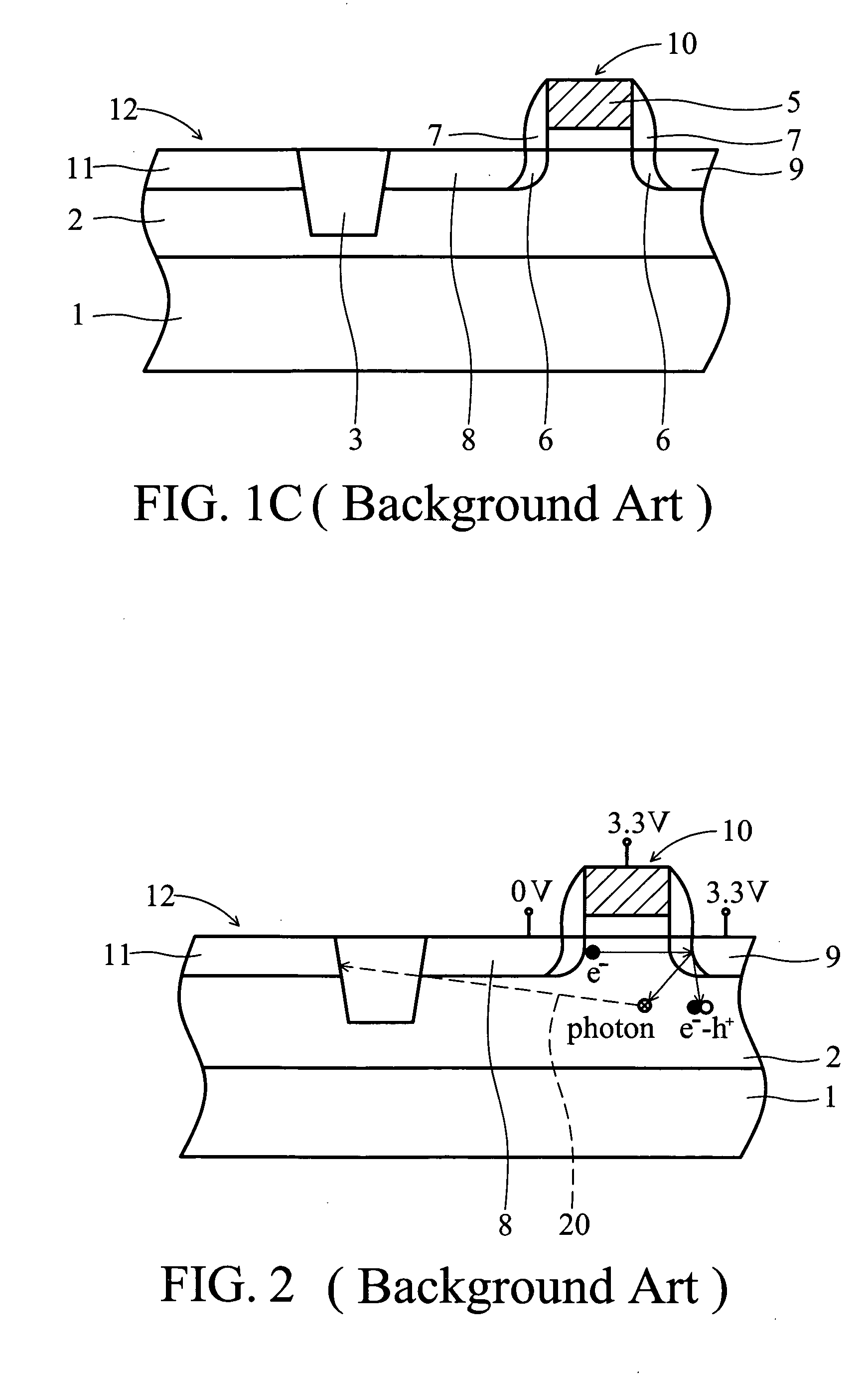
[0031] In FIG. 3A, a semiconductor substrate 100 is provided. The semiconductor substrate 100 may be a monocrystalline silicon substrate or a p-type substrate comprising single crystalline silicon with a crystallographic orientation. A shallow trench isolation (STI) structure 104 consisting of insulating material, e.g., such as SiO2, is formed in the substrate 100 by known isolation techniques. A relevant process for forming the shallow trench isolation s...

second embodiment

[0043]FIGS. 4A-4E are sectional views of an image sensor device according to an embodiment of the present invention and showing a method of manufacturing the image sensor device integrated with an LED of the present invention. In FIG. 4A, a semiconductor substrate 100 is provided. The semiconductor substrate 100 may be a monocrystalline silicon substrate or a p-type substrate comprised of single crystalline silicon with a crystallographic orientation. A shallow trench isolation (STI) structure 104 consisting of insulating material, e.g., such as SiO2, is formed in the substrate 100 by known isolation techniques. Formation of the shallow trench isolation structure 104 is described in, for example, U.S. Pat. No. 6,372,603, the entirety of which is hereby incorporated by reference, and is therefore not discussed herein to avoid obscuring aspects of the present invention. A p-well region 108 (serving as a diode well) is next formed in a top portion of the substrate 100 and in the pixel...


PUM


Abstract

An image sensor device and fabrication method thereof wherein a substrate having at least one shallow trench isolation structure therein is provided. At least one photosensor and at least one light emitting element, e.g., such as MOS or LED, are formed in the substrate. The photosensor and the light emitting element are isolated by the shallow trench isolation structure. An opening is formed in the shallow trench isolation structure to expose part of the substrate. An opaque shield is formed in the opening to prevent photons from the light emitting element from striking the photosensor.

Description

BACKGROUND OF THE INVENTION [0001] 1. Field of the Invention [0002] The present invention relates to an image sensor device and fabrication method thereof, and more particularly, to a method of forming optical guard rings for an image sensor device to eliminate interference between photodiode and adjacent light emitting structures. [0003] 2. Description of the Related Art [0004] Light imaging array devices are used in a wide variety of applications in the background art. These devices utilize an array of active pixels or image sensor cells. The image sensor cells usually include active image sensing elements, such as photodiodes, in addition to adjacent transistor structures, such as transfer gate structures, and reset transistors. These transistors, as well as additional devices used for control and signal circuits in the peripheral regions of the image sensor cell, or for peripheral logic circuits, include complimentary metal oxide semiconductor (CMOS) devices. [0005]FIGS. 1A-1C a...

Claims


Application Information

Patent Timeline
IPC IPC(8): H01L25/16H01L27/146H01L27/148H01L27/15
CPCH01L25/167H01L27/1462H01L27/14625H01L27/15H01L27/14687H01L27/14689H01L27/1463H01L2924/0002
Inventor HSU, TZU-HSUANYAUNG, DUN-NIANFANG, YEAN-KUEN
Owner TAIWAN SEMICON MFG CO LTD
Why Eureka
Try Eureka