Semiconductor memory device

a memory device and semiconductor technology, applied in the field of semiconductor memory devices, can solve the problems of large overhead of operation incidental to memory access, large number of steps, and disadvantages of the above method of the related art, and achieve the effect of effectively relieved defects, increased power consumption, and effective relief of defects in small units

Active Publication Date: 2005-12-22
SONY CORP
View PDF1 Cites 30 Cited by
  • Summary
  • Abstract
  • Description
  • Claims
  • Application Information

AI Technical Summary

Benefits of technology

[0039] Therefore, it is desired to provide a semiconductor memory device capable of flexibly relieving a defect of a memory and suppressing an access delay and an increase of a power consumption brought by the defect relieving.
[0066] According to the present invention, it is possible to flexibly relieve a defect of a memory, and an access delay and an increase of a power consumption brought by the defect relieving can be suppressed.

Problems solved by technology

The above method of the related art, however, suffers from disadvantages as below.
The first disadvantage is that a load on the host apparatus and an overhead of an operation incidental to a memory access are large.
Also, at the time of data accessing, a large number of steps have to be performed by the host apparatus.

Method used


Image

  • Semiconductor memory device
  • Semiconductor memory device
  • Semiconductor memory device

Examples


first embodiment

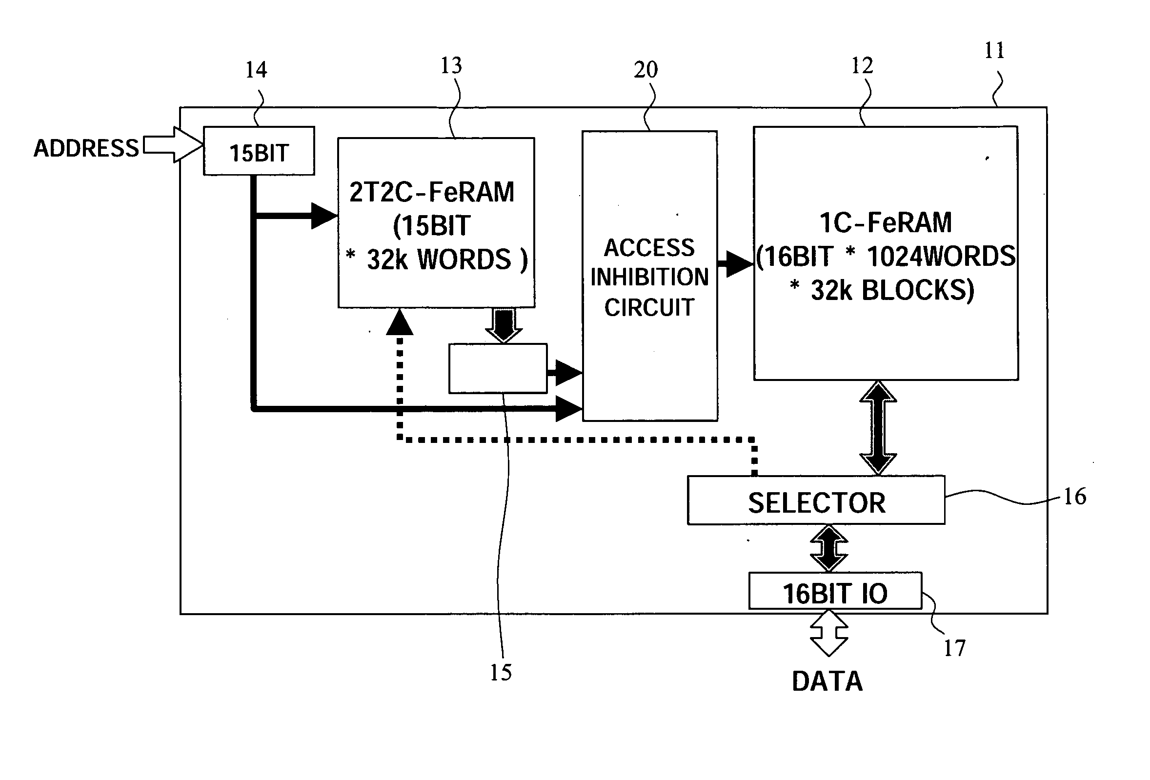
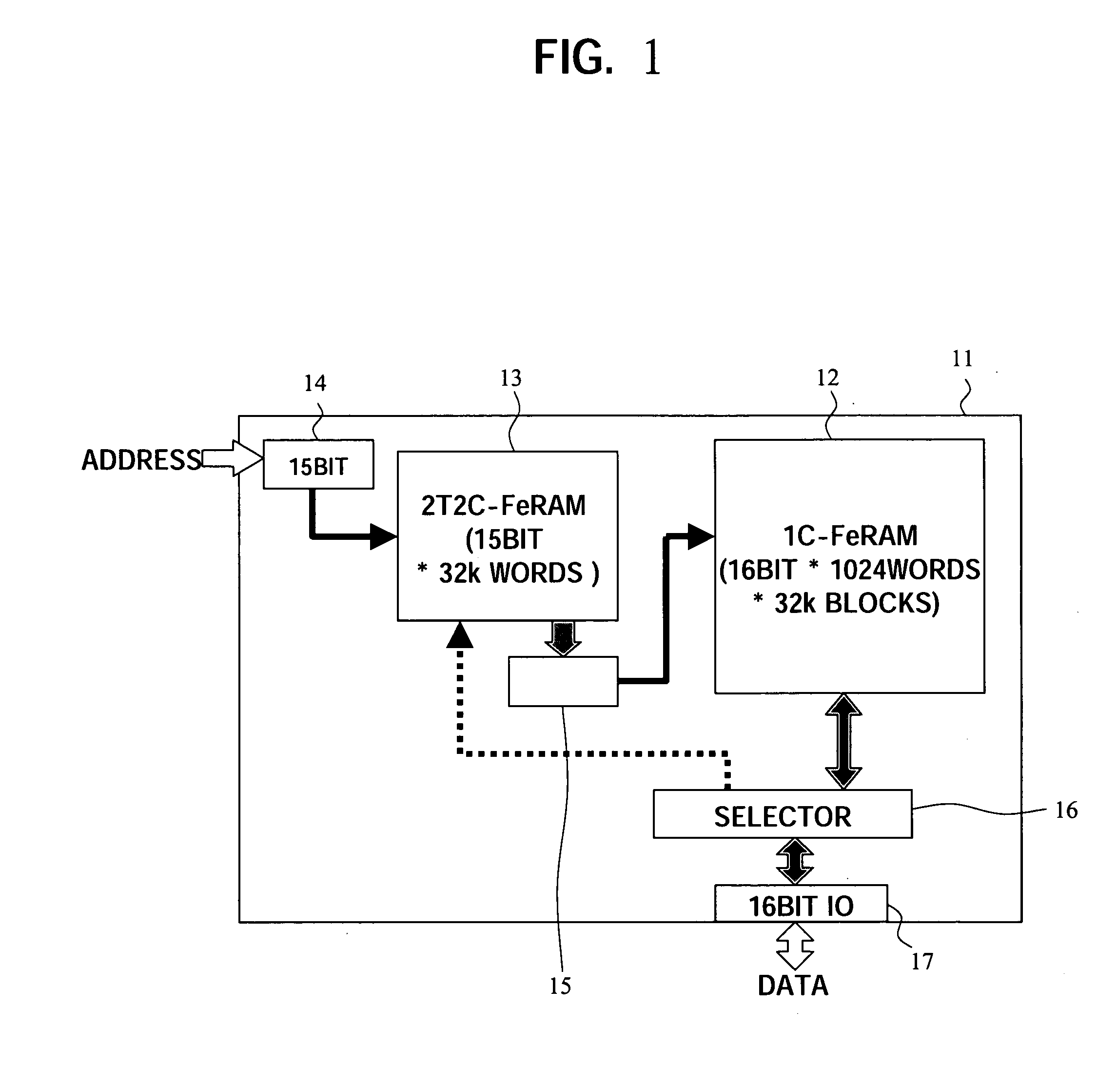
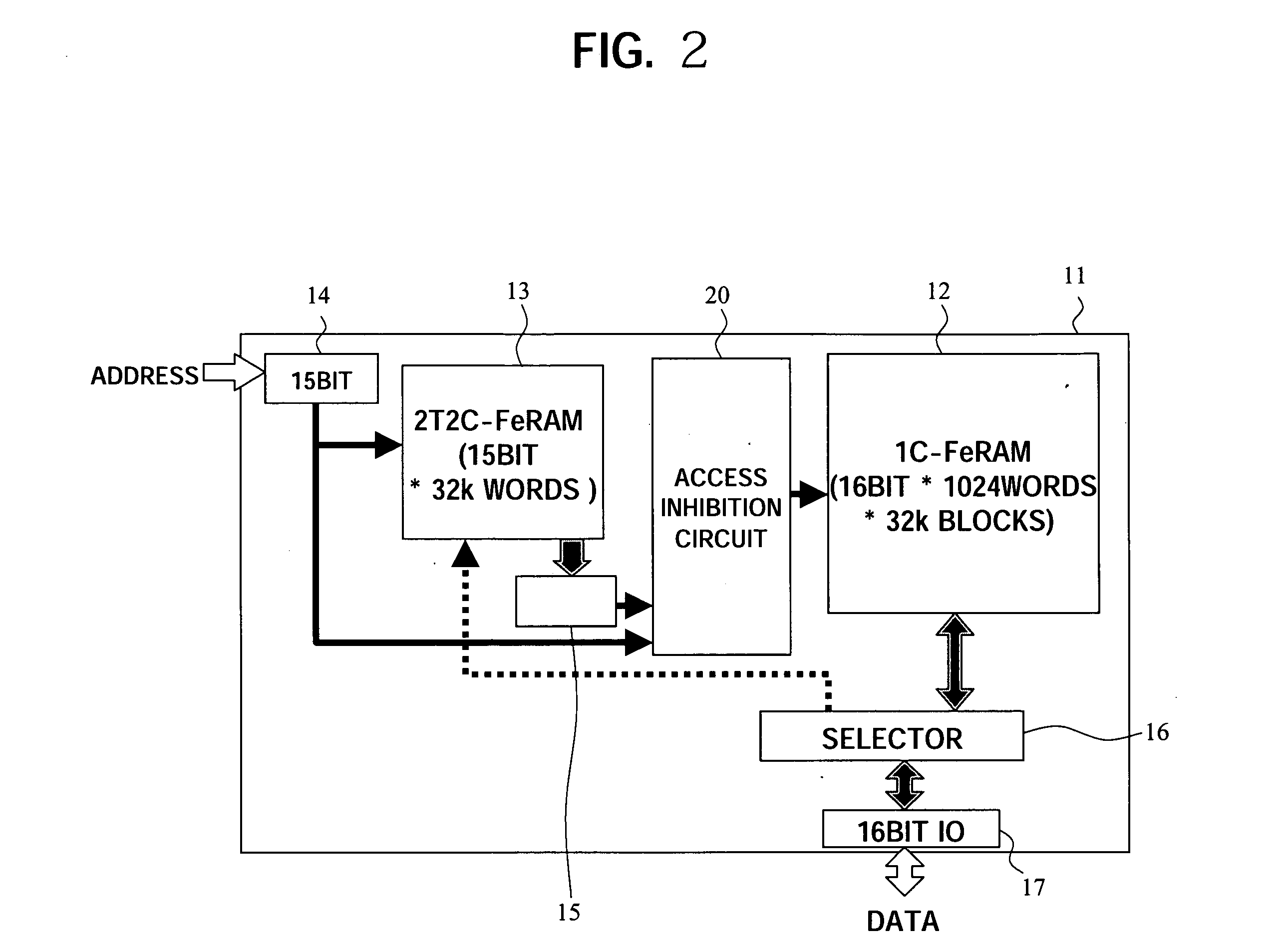
[0078]FIG. 1 is a view of an example of the configuration of a semiconductor memory device according to a first embodiment of the present invention.

[0079] The semiconductor memory device shown in FIG. 1 includes a first memory portion 12, a second memory portion 13, registers 14 and 15, a selector 16 and an input / output circuit 17, formed on a same semiconductor chip 11.

[0080] Note that the first memory portion 12 is an embodiment of a first memory portion of the present invention.

[0081] The second memory portion 13 is an embodiment of a second memory portion of the present invention.

[0082] A circuit including the register 14 is an embodiment of a first circuit of the present invention.

[0083] A circuit including the register 15 is an embodiment of a second embodiment of the present invention.

[0084] The first memory portion 12 is a memory portion corresponding to a body memory for storing user data and is composed of memory blocks by the number of about 32k in the present embod...

second embodiment

[0118] Next, a second embodiment of the present invention will be explained.

[0119]FIG. 3 is a view of an example of the configuration of a semiconductor memory device according to the second embodiment of the present invention.

[0120] The semiconductor memory device shown in FIG. 3 includes a first memory portion 12B, a second memory portion 13B, a third memory portion 18B, registers 14B, 15B and 19B, a selector 16B and an input / output circuit 17B, formed on the same semiconductor chip 11B.

[0121] Note that the first memory portion 12B is an embodiment of a first memory portion of the present invention.

[0122] The second memory portion 13B is an embodiment of a second memory portion of the present invention.

[0123] The third memory portion 18B is an embodiment of a third memory portion of the present invention.

[0124] A circuit including the register 14B is an embodiment of a first circuit of the present invention.

[0125] A circuit including the register 15B is an embodiment of a s...

third embodiment

[0154] Next, a third embodiment of the present invention will be explained.

[0155]FIG. 4 is a view of an example of the configuration of a semiconductor memory device according to the third embodiment of the present invention.

[0156] The semiconductor memory device shown in FIG. 4 includes a first memory portion 12C, a second memory portion 13C, registers 14C, 15C and 19C, a selector 16C and an input / output circuit 17C, formed on the same semiconductor chip 11C.

[0157] Note that the first memory portion 12C is an embodiment of a first memory portion of the present invention.

[0158] The second memory portion 13C is an embodiment of a second memory portion of the present invention.

[0159] A circuit including the register 14C is a first circuit according to embodiment of the present invention.

[0160] A circuit including the register 15C is a second circuit according to embodiment of the present invention.

[0161] The first memory portion 12C is a memory portion corresponding to a body m...


PUM


Abstract

A semiconductor memory device capable of flexibly relieving a defect of a memory and suppressing an access delay and an increase of a power consumption caused by defect relieving is provided, wherein an access to a first memory portion is made by referring to an address transformation table stored in a second memory portion, so that an access to a defective block is prevented; the second memory portion and the first memory portion are mounted on the same semiconductor chip, so that a part or all of address data input from outside the semiconductor chip can be made corresponding as it is to an address of the second memory portion and input to the second memory portion without executing any calculation, and a stored pointer can be taken out at a high speed; and an access can be made to a memory at a high speed by following the address transformation table without driving a system bus and a control line, which gives a heavy load, provided outside of the semiconductor chip or giving a load of processing on the CPU.

Description

CROSS REFERENCES TO RELATED APPLICATIONS [0001] The present invention contains subject matter related to Japanese Patent Application No. 2004-168679 filed in the Japanese Patent Office on Jun. 7, 2004, the entire contents of which being incorporated herein by reference. BACKGROUND OF THE INVENTION [0002] 1. Field of the Invention [0003] The present invention relates to a semiconductor memory device having a function of inhibiting an access to a memory region having a defect. [0004] 2. Description of the Related Art [0005] In recent years, along with a development of semiconductor fine processing technologies, a remarkable development has been made to attain a larger capacity of a semiconductor memory. For example, a flash memory for storing files has already reached a capacity of 1G bits and is still under development of a larger capacity. On the other hand, however, a large number of defect points also arise. Particularly when making a memory cell finer, an effect of microscopic un...

Claims


Application Information

Patent Timeline
Patent Type & Authority Applications(United States)
IPC IPC(8): G11C11/22G06F11/00G11C7/00G11C29/00G11C29/04G11C29/42
CPCG11C29/76G11C29/00
Inventor NISHIHARA, TOSHIYUKI
Owner SONY CORP
Why Eureka
Try Eureka