Semiconductor light emitting element, semiconductor light emitting device, and method for fabricating semiconductor light emitting element

a light emitting element and semiconductor technology, applied in the direction of optical elements, instruments, optics, etc., can solve the problems of difficult formation of ohmic electrodes, reduced power conversion efficiency, and increased contact resistance, so as to facilitate micro-processing, facilitate micro-processing, and improve light extraction efficiency

Inactive Publication Date: 2005-12-29
PANASONIC CORP
View PDF3 Cites 135 Cited by
  • Summary
  • Abstract
  • Description
  • Claims
  • Application Information

AI Technical Summary

Benefits of technology

[0015] The surface of the LED in which a two-dimensional photonic crystal can conceivably be formed is the main or back surface thereof. In this case, the back surface of the substrate and the interface between the substrate and the semiconductor can be considered as two locations at either of which the photonic crystal is to be formed. In either case, however, the following problem is encountered when the photonic crystal is formed by using the conventional technology. In the case of forming the photonic crystal at the back surface of the substrate, total reflection occurs at the interface between the semiconductor and the substrate so that the effect of improving the light extraction efficiency achieved by the photonic crystal formed in the back surface of the substrate is lower than when the photonic crystal is formed in the semiconductor. In the case of forming the photonic crystal at the interface between the semiconductor and the substrate, on the other hand, the efficiency of diffraction by the periodic projections / depressions lowers due to a small refractive index difference between the semiconductor and the substrate so that the effect of improving the light extraction efficiency is lower than when the photonic crystal is formed at the uppermost surface of the LED.
[0047] The method further comprises the steps of: mounting the semiconductor light emitting element on a mounting substrate; and molding the semiconductor light emitting element with a hemispherical resin by using a mold die formed with a hemispherical cavity. The arrangement allows the fabrication of the semiconductor light emitting element with higher light extraction efficiency. By molding the resin by using the mold die, it becomes possible to stably manufacture semiconductor light emitting elements having uniform configurations.

Problems solved by technology

However, there are cases where the following problems occur when projections / depressions are formed in the surface of the LED close to the active layer, such as in the p-type GaN layer.
As a result, there are cases where the series resistance of a conventional LED as shown in FIG. 35 increases and the power conversion efficiency thereof lowers.
In the p-type GaN layer 1004, however, the crystal defect resulting from an etching damage compensates for the holes so that the formation of an ohmic electrode becomes difficult.
This leads to the problem that the contact resistivity increases and the power conversion efficiency lowers.
Since the projections / depressions are close to the active layer, etching-induced damage occurs in the active layer during the formation of the projections / depressions.
Consequently, the problems of a reduction in internal quantum efficiency (the ratio of electron-hole pairs that are recombined in the active layer and converted to photons to all the electron-hole pairs recombined in the active layer) in the active layer and a reduction in the light emission efficiency of the LED are also likely to occur.
In either case, however, the following problem is encountered when the photonic crystal is formed by using the conventional technology.

Method used


Image

  • Semiconductor light emitting element, semiconductor light emitting device, and method for fabricating semiconductor light emitting element
  • Semiconductor light emitting element, semiconductor light emitting device, and method for fabricating semiconductor light emitting element
  • Semiconductor light emitting element, semiconductor light emitting device, and method for fabricating semiconductor light emitting element

Examples


embodiment 1

Structure of Light Emitting Element

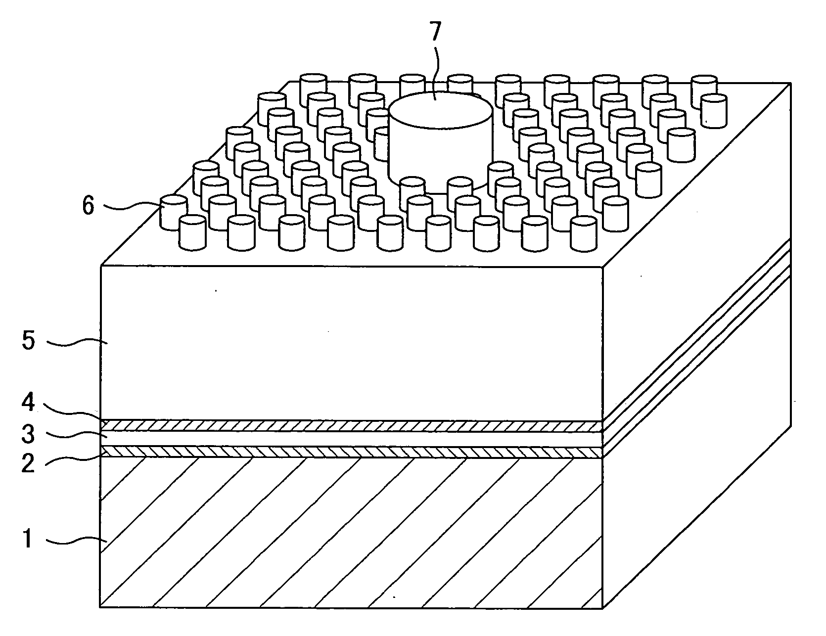
[0084]FIG. 1 is a perspective view showing a semiconductor light emitting element according to a first embodiment of the present invention. As shown in the drawing, the semiconductor light emitting element according to the present embodiment comprises: a p-type GaN layer (first semiconductor layer) 3 formed by epitaxial growth and having a thickness of 200 nm; a high-reflection p electrode (first electrode) 2 formed on the crystal growing surface (principal surface) of the p-type GaN layer 3, made of platinum (Pt) and gold (Au) which are stacked in layers, and having a thickness of 1 μm; an Au plating layer 1 formed on the lower surface of the high-reflection p electrode 2 and having a thickness of 10 μm; a non-doped InGaN active layer 4 formed on the back surface of the p-type GaN layer 3 and having a thickness of 3 nm; an n-type GaN layer (second semiconductor layer) 5 formed on the back surface of the non-doped InGaN active layer 4, having a b...

embodiment 2

[0126]FIG. 18A is a perspective view showing a semiconductor light emitting element according to a second embodiment of the present invention. FIG. 18B is a plan view when the semiconductor light emitting element according to the second embodiment is viewed from above. The semiconductor light emitting element according to the present embodiment is different from the semiconductor light emitting element according to the first embodiment in that a projecting two-dimensional periodic structure 18 formed in the upper surface (back surface) of the n-type GaN layer 5 is configured as polygonal pyramids.

[0127] As shown in FIGS. 18A and 18B, the semiconductor light emitting element according to the present embodiment comprises: the p-type GaN layer 3 formed by epitaxial growth and having a thickness of 200 nm; the high-reflection p electrode 2 formed on the crystal growing surface of the p-type GaN layer 3, made of platinum (Pt) and gold (Au) which are stacked in layers, and having a thick...

embodiment 3

[0143]FIG. 26 is a perspective view showing a semiconductor light emitting device according to a third embodiment of the present invention. The semiconductor light emitting device according to the present embodiment is a resin-molded semiconductor light emitting device obtained by mounting the semiconductor light emitting element according to the first or second embodiment on a mounting substrate 22 and then molding the periphery of the light emitting element with a hemispherical dome-shaped resin 23. In FIG. 26, those of the components of the semiconductor light emitting element which are the same as shown in FIG. 1 are designated by the same reference numerals.

[0144] By thus molding the light emitting element with the dome-shaped resin, the light extraction efficiency of the semiconductor light emitting element can be improved, as will be described herein below.

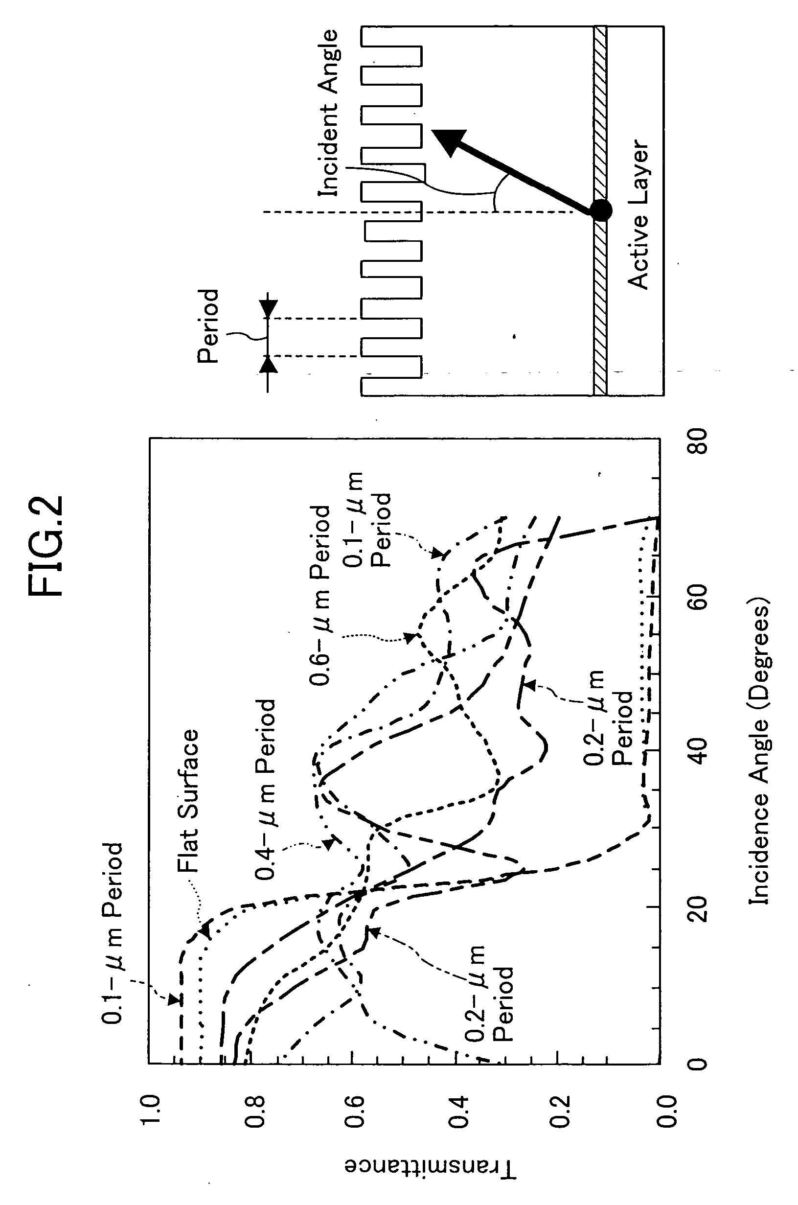
[0145]FIG. 27A is a view showing the result of theoretically calculating the transmittance of light when the semiconduc...


PUM


Abstract

Projections / depressions forming a two-dimensional periodic structure are formed in a surface of a semiconductor multilayer film opposing the principal surface thereof, while a metal electrode with a high reflectivity is formed on the other surface. By using the diffracting effect of the two-dimensional periodic structure, the efficiency of light extraction from the surface formed with the projections / depressions can be improved. By reflecting light emitted toward the metal electrode to the surface formed with the projections / depressions by using the metal electrode with the high reflectivity, the foregoing effect achieved by the two-dimensional periodic structure can be multiplied.

Description

CROSS REFERENCE TO RELATED APPLICATIONS [0001] The present application claims priority under 35 U.S.C. § 119(a) to Japanese Patent Application JP 2004-189892, filed Jun. 28, 2004, the entire content of which is incorporated herein by reference. BACKGROUND OF THE INVENTION [0002] 1. Technical Field to which the Invention Pertains [0003] The present invention relates to a light emitting element using a semiconductor and to a method for fabricating the same. [0004] 2. Prior Art [0005] The use of a nitride-based compound semiconductor represented by AlInGaN has enabled the commercialization of light emitting elements which output light at the ultraviolet, blue, and green wavelengths from which it has heretofore been difficult to obtain a sufficient emission intensity, such as a light emitting diode (LED) and a semiconductor laser, so that research and development thereof has been conducted vigorously. Among light-emitting elements, an LED is easier to fabricate and control than a semico...

Claims


Application Information

Patent Timeline
Patent Type & Authority Applications(United States)
IPC IPC(8): G02B6/122H01L33/32H01L29/22H01L33/20H01L33/40H01L33/54H01L33/56H01L33/62
CPCB82Y20/00G02B6/1225H01L33/20H01L2933/0083H01L33/42H01L33/54H01L33/22
Inventor ORITA, KENJI
Owner PANASONIC CORP
Why Eureka
Try Eureka