Light-emitting device

a light-emitting device and high-efficiency technology, applied in the direction of semiconductor devices, basic electric elements, electrical appliances, etc., can solve the problems of increasing operation voltage, achieve the effect of reducing both the total reflection effect on the device surface and the light absorption effect, improving the light-emitting efficiency of the device, and reducing the total reflection

Active Publication Date: 2005-12-29
EPISTAR CORP
View PDF11 Cites 54 Cited by
  • Summary
  • Abstract
  • Description
  • Claims
  • Application Information

AI Technical Summary

Benefits of technology

[0015] Furthermore, the other advantages of the claimed invention of the hexagonal-pyramid cavities are that the hexagonal-pyramid cavities can effectively reduce both the total reflection effect on the device surface and the light absorption effect of the p-type nitride semiconductor stack. Thus the light-emitting ef

Problems solved by technology

In general, if the second nitride semiconductor stack is p-type material and its surface opposite to the nitride light-emitting layer is flat smooth, and parallel to the substrate

Method used


Image

  • Light-emitting device
  • Light-emitting device
  • Light-emitting device

Examples


second embodiment

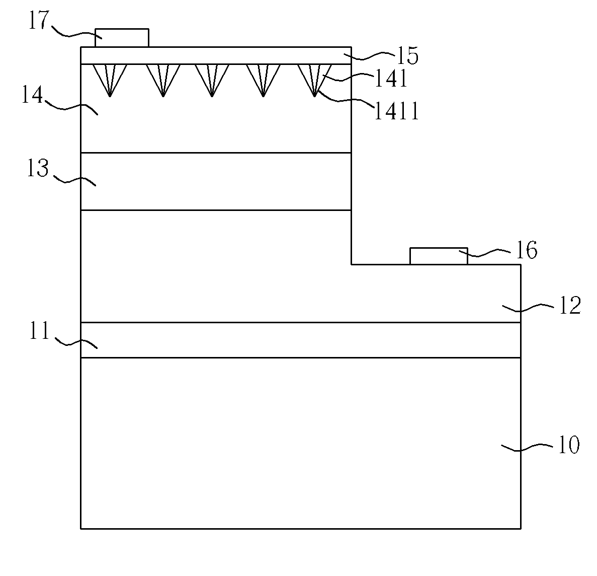
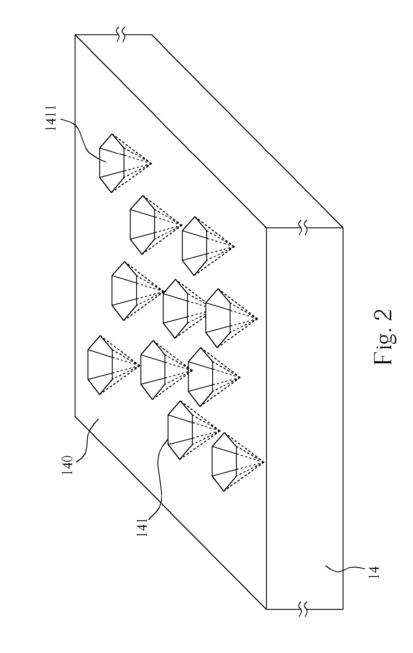
[0046] Please refer to FIG. 9, which is a diagram of the light-emitting device according to the present invention. The second surface of the n-type nitride semiconductor stack 12 of the light-emitting device further comprises an n-type electrode contact area 121 and a non-electrode contact area 122. The n-type electrode 16 is formed on the n-type electrode contact area 121. The non-electrode contact area 122 further includes a high-efficiency light-emitting surface. A rough surface or a plurality of hexagonal-pyramid cavities is formed by performing an etching process or epitaxial growth on the high-efficiency light-emitting surface. In this embodiment, the light-emitting device includes a rough surface 123. Because of the rough surface 123 of the non-electrode contact area 122, lateral light reflected between the substrate 10 and the n-type nitride semiconductor stack 12 can be reduced, so that the lateral light can be emitted effectively for increasing the light-emitting efficienc...

third embodiment

[0047] Please refer to FIG. 10, which is a diagram of the light-emitting device according to the present invention. The light-emitting device further comprises a second transparent conductive oxide layer 18 formed on the rough surface 123 and the non-electrode contact area 122; also, the second transparent conductive oxide layer 18 contacts with the n-type electrode 16, such that current spreading at the second transparent conductive oxide layer 18 is better. Moreover, the light-emitting efficiency is improved if the refractive index of the second transparent conductive oxide layer 18 is between the refractive indexes of nitride material and package material.

[0048] In the above-mentioned embodiments, a transparent conductive oxide layer can be formed between the n-type electrode 16 and the n-type electrode contact area 121 of the second surface of the n-type nitride semiconductor stack 12.

[0049] In the above-mentioned embodiments, the transparent conductive oxide layer can be taken...


PUM


Abstract

A light-emitting device includes a substrate, a first nitride semiconductor stack formed on the substrate, a nitride light-emitting layer formed on the first nitride semiconductor stack, a second nitride semiconductor stack formed on the nitride light-emitting layer, and a first transparent conductive oxide layer formed on the second nitride semiconductor stack. The second nitride semiconductor stack includes a plurality of hexagonal-pyramid cavities formed in an upper surface of the second nitride semiconductor stack. The plurality of hexagonal-pyramid cavities of the second nitride semiconductor stack are filled with the first transparent conductive oxide layer, and a low-resistance ohmic contact is generated at the inner surfaces of the plurality of hexagonal-pyramid cavities so as to decrease the operation voltage and improve light-emitting efficiency of the light-emitting device.

Description

BACKGROUND OF THE INVENTION [0001] 1. Field of the Invention [0002] The present invention relates to a light-emitting device, and more particularly, to a high efficiency light-emitting device. [0003] 2. Description of the Prior Art [0004] Semiconductor light-emitting devices have been applied widely in optical display devices, traffic signals, data storing devices, communication devices, illumination devices, and medical apparatuses. [0005] The conventional nitride LED includes a thin metallic layer on a top surface of the LED, such as material of the Ni / Au group, regarded as a transparent conductive layer. However, part of LED light still cannot travel through metal. Light generated by the LED is absorbed by the thin metallic layer and the light transmittance is decreased. In order to have a good transmittance, the thickness of the thin metallic layer is limited to be within several tens to several hundreds of angstroms. Although the thickness of the thin metallic layer is limited,...

Claims


Application Information

Patent Timeline
IPC IPC(8): H01L31/00H01L33/22
CPCH01L33/22
Inventor OU, CHENLIN, TING-YANGLAI, SHIH-KUO
Owner EPISTAR CORP
Why Eureka
Try Eureka