Semiconductor device and method of manufacturing same

a semiconductor and semiconductor technology, applied in the direction of semiconductor devices, electrical devices, transistors, etc., can solve the problems of difficult local stress application to soi devices, limited application range of soi technology, and self-heating problems of devices formed on silicon layers, etc., to achieve effective address the floating effect of substrates, reduce junction resistance, and increase carrier mobility

Inactive Publication Date: 2005-12-29
SAMSUNG ELECTRONICS CO LTD
View PDF5 Cites 63 Cited by
  • Summary
  • Abstract
  • Description
  • Claims
  • Application Information

AI Technical Summary

Benefits of technology

[0013] According to the present invention, the short channel effect is constrained and junction resistance is reduced by forming the spaces in the active region below the gate electrode. Furthermore, it effectively addresses...

Problems solved by technology

Unfortunately, however, a substrate floating effect may occur in MOS transistors formed on an SOI substrate where an element in a channel region assumes a floating state electric potential.
Furthermore, where a buried oxide layer (BOX) is formed below a silicon substrate, a self-heating problem often occurs in devices formed on the silicon layer.
As a result, the range ...

Method used


Image

  • Semiconductor device and method of manufacturing same
  • Semiconductor device and method of manufacturing same
  • Semiconductor device and method of manufacturing same

Examples


Embodiment Construction

[0021] Exemplary embodiments of the invention are described below with reference to the corresponding drawings. These embodiments are presented as teaching examples. The actual scope of the invention is defined by the claims that follow.

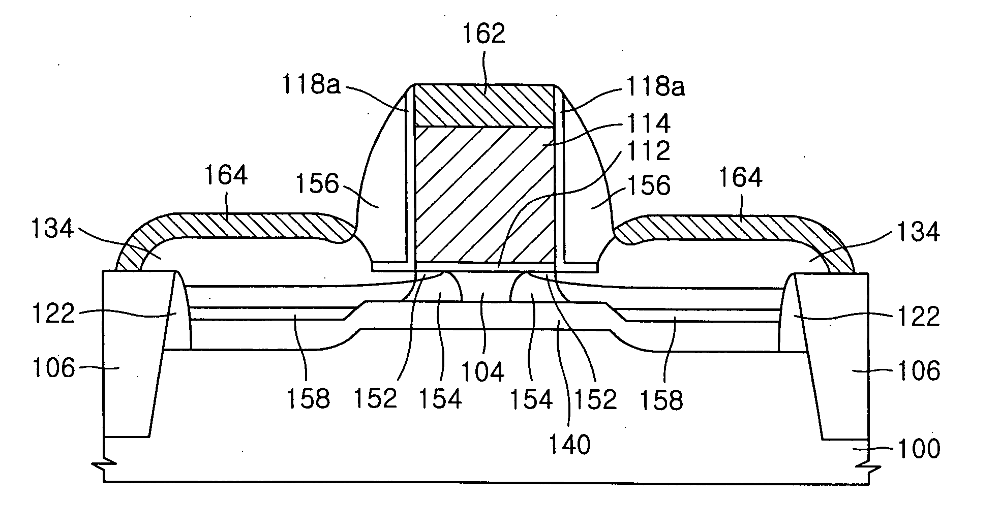
[0022]FIGS. 1A through 1M are cross-sectional views illustrating a method of manufacturing a semiconductor device according to one embodiment of the present invention.

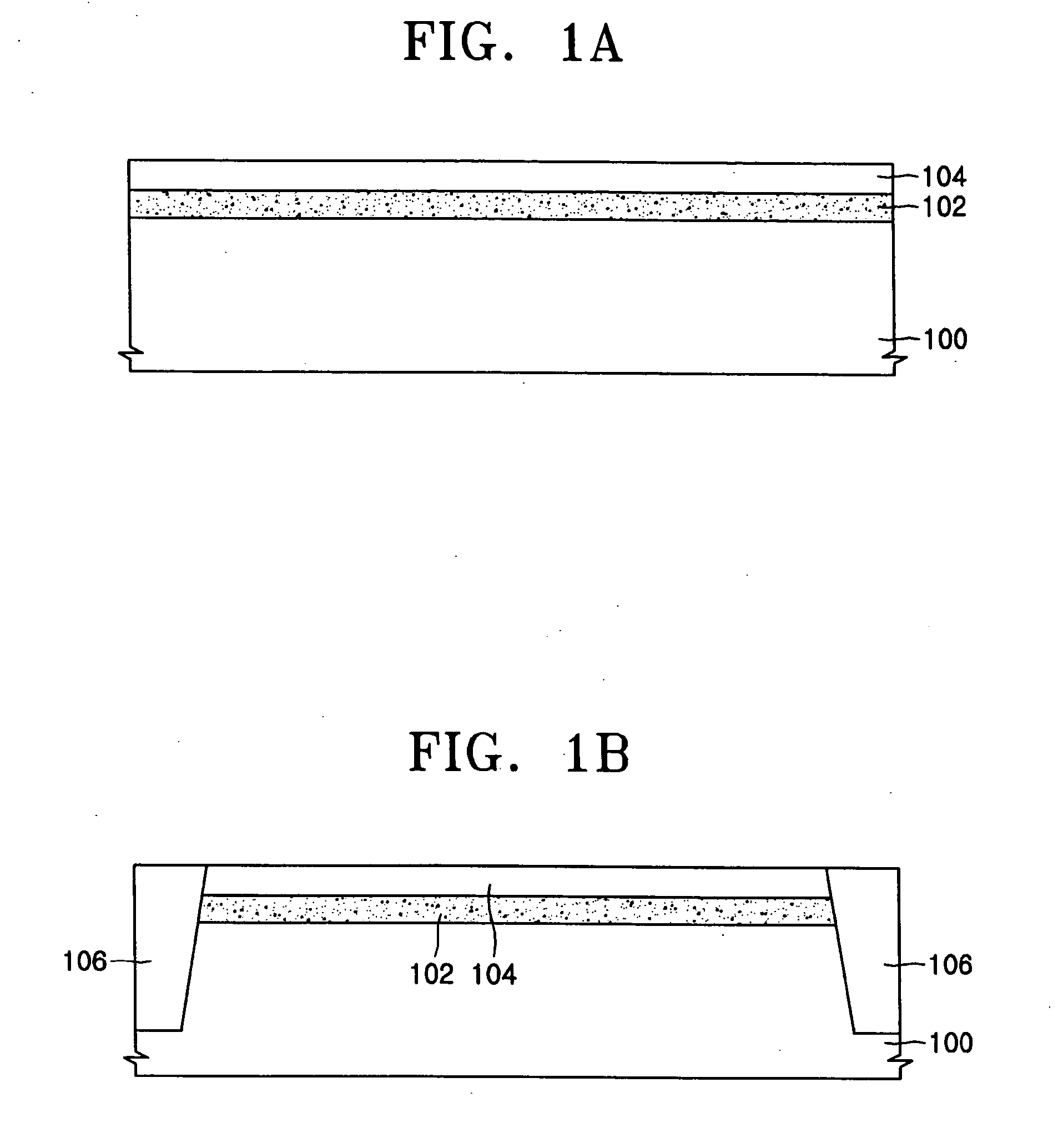
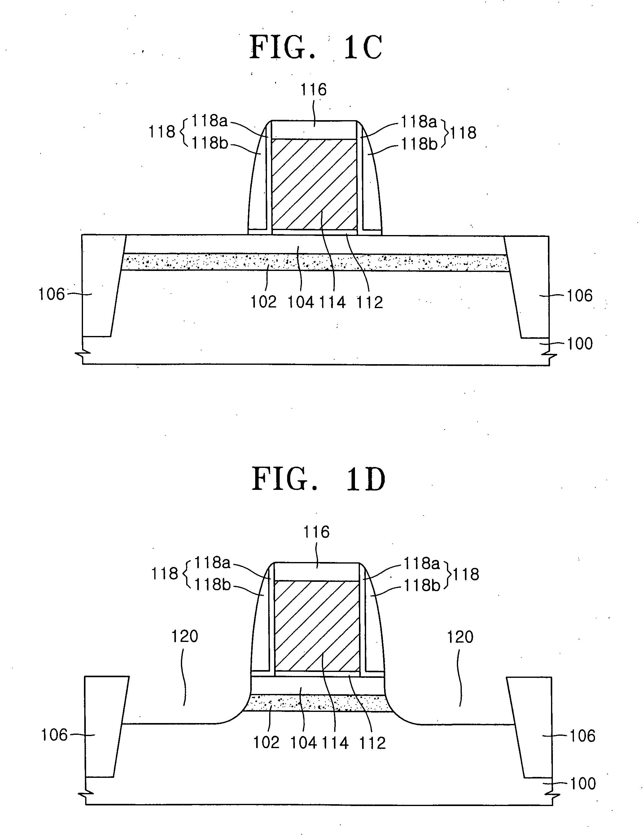
[0023] Referring to FIG. 1A, a first silicon germanium (SiGe) layer 102 is formed on a bulk semiconductor substrate 100 such as a silicon substrate. First SiGe layer 102 is generally formed to a thickness of about 10 to 100 nm using a selective epitaxial growth technology. A silicon (Si) layer 104 is then formed on first SiGe layer 102 to a thickness of about 5 to 50 nm.

[0024] Referring to FIG. 1B, an active region is defined by forming a device isolation region 106 on semiconductor substrate 100 using a conventional isolation method such as a trench isolation method. In other words,...


PUM


Abstract

A semiconductor device and related method of manufacture are disclosed. The semiconductor device comprises a gate electrode formed on a semiconductor substrate, an active region containing spaces formed below the gate electrode, a channel region formed between the gate electrode and the spaces, and source and drain regions formed on opposite sides of the gate electrode within the active region. The spaces are formed by etching a semiconductor layer formed below the gate electrode in the active region.

Description

BACKGROUND OF THE INVENTION [0001] 1. Field of the Invention [0002] The present invention relates generally to a semiconductor device and a method of manufacturing the same. More particularly, the invention relates to a semiconductor device comprising a metal oxide semiconductor (MOS) transistor and a method of manufacturing the same. [0003] A claim of priority is made to Korean Patent Application No. 10-2004-0049004 filed on Jun. 28, 2004, the disclosure of which is hereby incorporated by reference in its entirety. [0004] 2. Description of the Related Art [0005] Fully depleted silicon-on-insulator (FD-SOI) technology has been widely used to create high speed, low power logic circuits. Using FD-SOI technology reduces parasitic capacitances associated with source, drain, and channel regions of semiconductor circuits, thereby allowing the circuits to operate at higher speeds. In addition, FD-SOI technology reduces the amount of leakage current occurring at source and drain junctions o...

Claims


Application Information

Patent Timeline
IPC IPC(8): H01L21/00H01L21/336H01L27/01H01L29/786
CPCH01L29/66772H01L29/78621H01L29/78687H01L29/78654H01L29/78639H01L29/7848
Inventor LEE, SUNG-YOUNGSHIN, DONG-SUK
Owner SAMSUNG ELECTRONICS CO LTD
Why Eureka
Try Eureka