Semiconductor package with exposed heat sink and the heat sink thereof

a technology of exposed heat sink and semiconductor package, which is applied in the direction of semiconductor/solid-state device details, semiconductor devices, electrical devices, etc., can solve the problems of insufficient heat dissipation efficiency, short heat dissipation path, and adverse effects on the performance of these devices, so as to ensure the heat dissipation efficiency of the semiconductor package and reduce the flow speed of the encapsulant

Inactive Publication Date: 2005-12-29
SILICONWARE PRECISION IND CO LTD
View PDF7 Cites 37 Cited by
  • Summary
  • Abstract
  • Description
  • Claims
  • Application Information

AI Technical Summary

Benefits of technology

[0015] During a molding process, when the encapsulant flows to the stepped structure, a flowing speed of the encapsulant is reduced due to a gradually decreased flow-accommodating space on the stepped structure, and the flow of encapsulant is further blocked by the side wall on the highest step surface of the stepped structure, such that any flash of t

Problems solved by technology

If the heat dissipation problem cannot be properly solved, the performances of these devices would be adversely affected.
This heat dissipating path is relatively lengthy and does not provide a sufficient heat dissipating efficiency.
The foregoing semiconductor package can desirably improve the heat dissipating efficiency thereof, however, it still has a drawback during a molding process of forming the encapsulant 14 in order to expose the surface 130 of the heat sink 13.
However, the surface 130 of the heat sink 13 may not be perfectly planar due to undesirable rolled portions being possibly formed at edges of the heat sink 13 fabricated by a stamping technique.
This not only impairs the appearance of the packaged product but also reduces the heat dissipating area and the heat dissipating efficiency.
If an additional deflash process is performed t

Method used


Image

  • Semiconductor package with exposed heat sink and the heat sink thereof
  • Semiconductor package with exposed heat sink and the heat sink thereof
  • Semiconductor package with exposed heat sink and the heat sink thereof

Examples


Embodiment Construction

[0029] The preferred embodiments of a semiconductor package with an exposed heat sink and the heat sink thereof proposed in the present invention are described in detail with reference to FIGS. 5A-5B, 6A-6B, 7, 8 and 9A-9B.

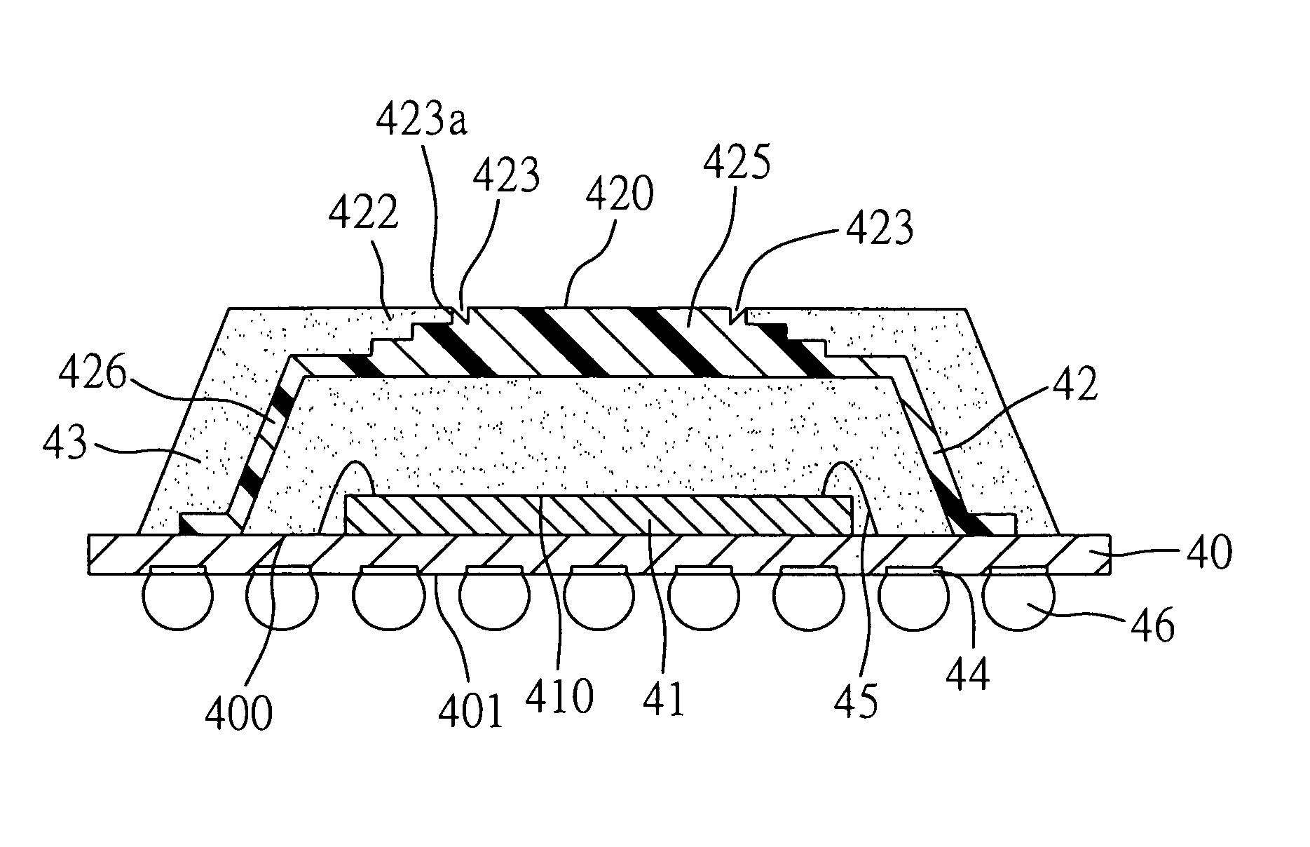
[0030] As shown in FIG. 5A, the semiconductor package according to a preferred embodiment of the present invention comprises: a substrate 40; a chip 41 attached to the substrate 40 via an adhesive (not shown); and a heat sink 42 mounted on the substrate 40 and covering the chip 41. The substrate 40 has a first surface 400 and a second surface 401 opposed to the first surface 400, wherein a first conductive trace layer is formed on the first surface 400, and a second conductive trace layer is formed on the second surface 401, such that the first conductive trace layer is electrically connected to the second conductive trace layer by a plurality of conductive vias (not shown) formed through the substrate 40. A plurality of ball pads 44 are provided at terminals of ...


PUM


Abstract

A semiconductor package with an exposed heat sink and the heat sink thereof are proposed. A carrier having a first surface and a second surface is provided. At least one chip is mounted on the first surface of the carrier and electrically connected to the carrier. A heat sink includes a flat portion having an exposed surface, and a support portion extended peripherally from the flat portion and attached to the first surface of the carrier, wherein the flat portion, the support portion and the carrier form a space where the chip is received, and the flat portion is peripherally formed with a stepped structure having at least one flash preventing groove located at a position adjacent to the exposed surface so as to prevent resin flashes on the exposed surface of the heat sink during a molding process for forming an encapsulant that encapsulates the chip.

Description

FIELD OF THE INVENTION [0001] The present invention relates to semiconductor packages with exposed heat sinks and the heat sinks thereof, and more particularly, to a ball grid array (BGA) semiconductor package having an exposed heat sink for preventing resin flashes, and the heat sink of the semiconductor package. BACKGROUND OF THE INVENTION [0002] The advancement of the semiconductor technology has raised the requirements of processing speed and functionality for chips, which induces a concern of how to effectively dissipate heat produced during operation of the chips so as to assure the reliability of semiconductor devices where the chips are incorporated. For example, a ball grid array (BGA) semiconductor package is usually used with devices having a large number of input / output (I / O) connections for highly integrated chips, such as 2D or 3D graphic chip, chip set, central processing unit (CPU), and memory, etc. If the heat dissipation problem cannot be properly solved, the perfo...

Claims


Application Information

Patent Timeline
IPC IPC(8): H01L21/56H01L23/10H01L23/31H01L23/433
CPCH01L21/565H01L23/3128H01L23/4334H01L24/48H01L2924/15311H01L2924/16152H01L2224/48227H01L2924/00014H01L2924/14H01L2924/181H01L2924/00H01L2924/00012H01L2224/45099H01L2224/45015H01L2924/207
Inventor CHEN, YEN-CHUNLIN, SUN-ZENCHANG, CHICH-YUAN
Owner SILICONWARE PRECISION IND CO LTD
Why Eureka
Try Eureka