

Process for manufacturing leadless semiconductor packages including an electrical test in a matrix of a leadless leadframe
- Summary
- Abstract
- Description
- Claims
- Application Information
AI Technical Summary
Benefits of technology
Problems solved by technology
Method used
Image

Examples
first embodiment
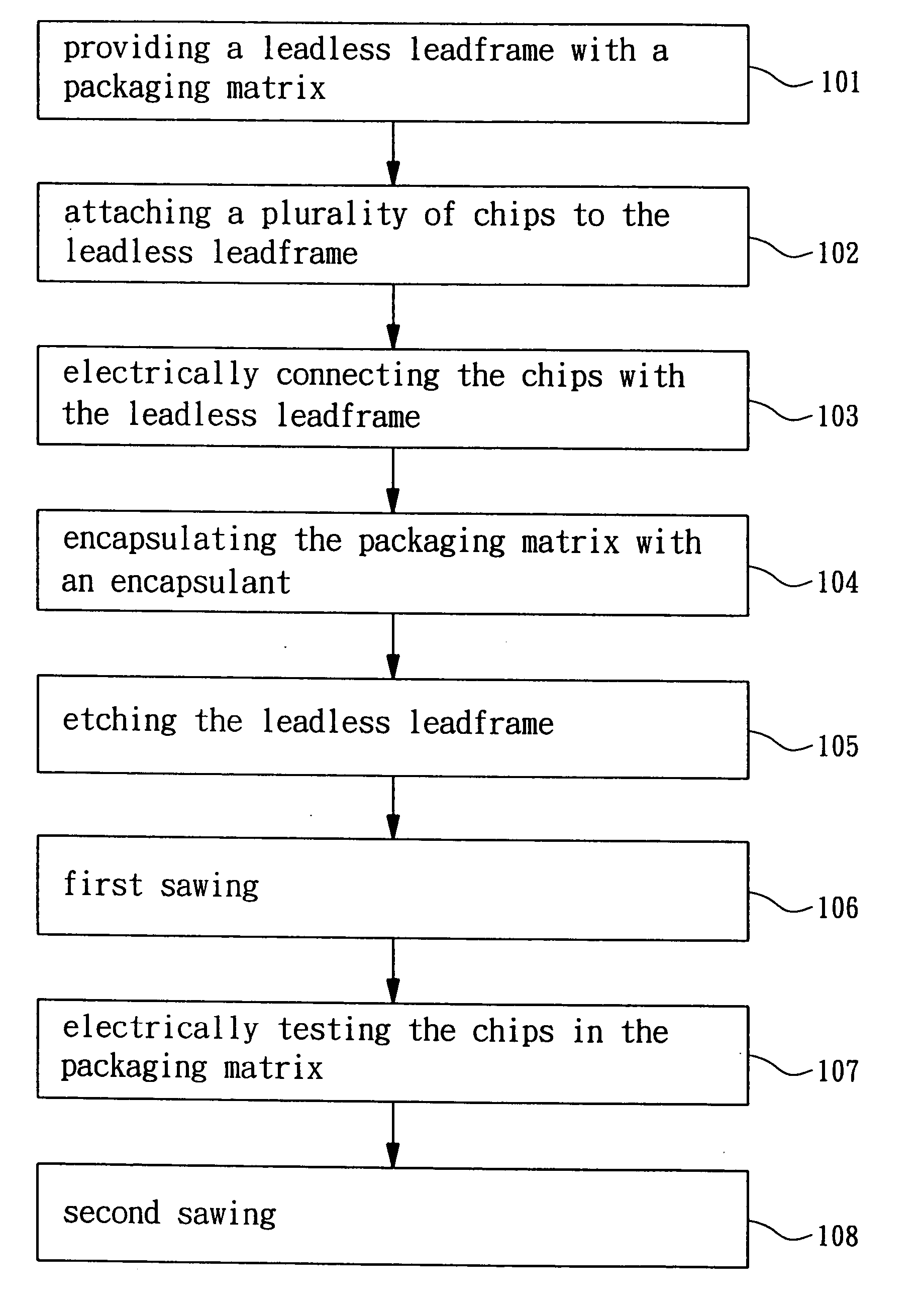
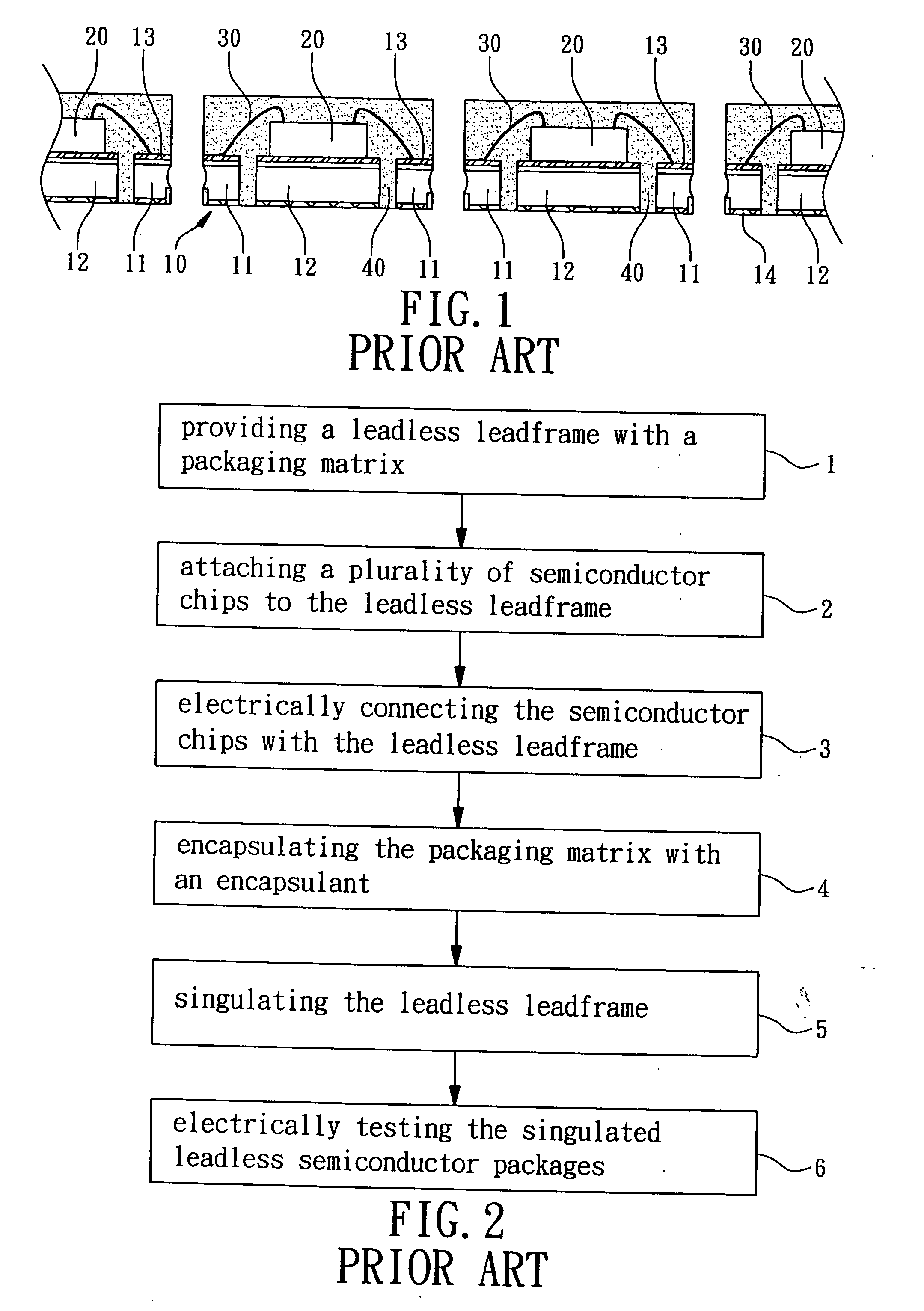
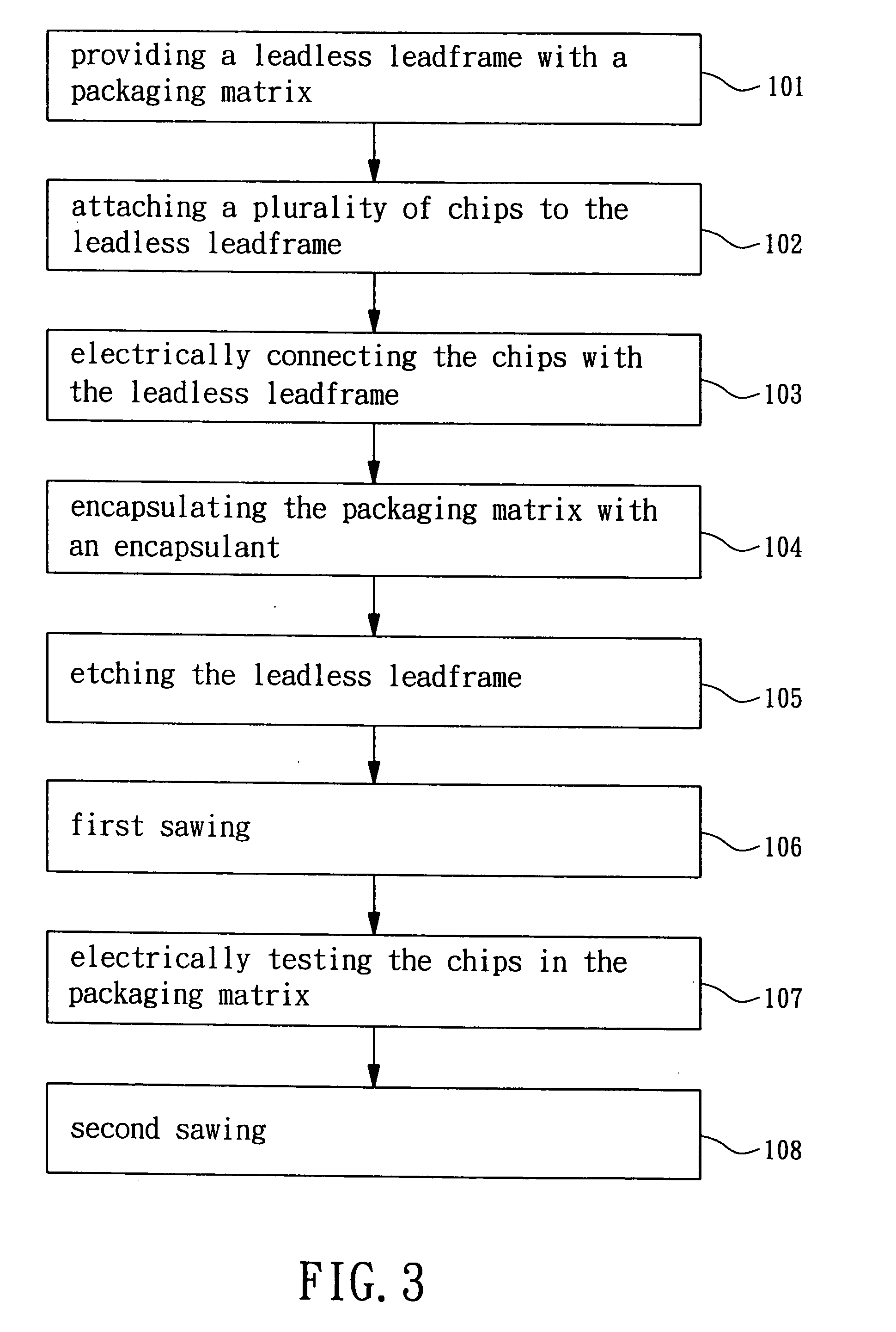
[0016] Accord to the present invention, firstly in the step 1, as shown in FIGS. 4A and 5, a leadless leadframe 110 with a packaging matrix 111 is provided such as a quad flat non-leaded (QFN) leadframe. The leadless leadframe is made of metal or metal alloy containing copper or iron. There is at least one packaging matrix 111 on the leadless leadframe 110, as shown in FIG. 5. In this embodiment, the leadless leadframe 110 has a plurality of packaging matrixes 111 in linear arrangement. Each packaging matrix 111 defines a plurality of units 112 and a plurality of cutting streets 113. Moreover, the leadless leadframe 110 has a plurality of leads 114 and a plurality of connecting bars 116. A plurality of leads 114 are arranged at the periphery of each unit 112. The plurality of connecting bars 116 are formed inside the packaging matrix 111 along the cutting streets 113 to connect the leads 114. In this embodiment, a plurality of the chip pads 115 are formed in the corresponding units ...
second embodiment
[0024] According to the present invention, as shown in FIG. 7A, another leadless leadframe 310 with a packaging matrix in step 101 is provided. There is at least a packaging matrix, not shown in the figure, in the leadless leadframe 310. The packaging matrix defines a plurality of units 311 and a plurality of cutting streets 312. Moreover, the leadless leadframe 310 has a plurality of leads 313 and a plurality of connecting bars 314. The leads 313 are formed in the units 311 and are connected with the connecting bars 314 along the cutting streets 312. A plated metal layer 315, such as gold-palladium-nickel-palladium or other unetchable metal layer, is deposited on the upper surface 313a of the leads 313 and the upper surface 314a of the connecting bars 314, preferably, an indentation 316 is formed on the lower surfaces 314b of the connecting bars 314 corresponding to the cutting streets 312. A back tape 410 is attached to the lower surface of the leadless leadframe 310. In the prese...
third embodiment
[0031] According to the present invention, a process for manufacturing a plurality of leadless semiconductor packages from a leadless leadframe having a packaging matrix includes the steps similar to the steps as shown in FIG. 3, except the chip-attaching step 102 and the wire-bonding step 103 are replaced with a flip-chip bonding step. Referring to FIGS. 3 and 8, a leadless leadframe 510 is provided in step 101, which has a packaging matrix including a plurality of leads 511 in each units and a plurality of connecting bars 512 between the units. The leads 511 are connected to the connecting bars 512. A plated metal layer 513 is formed on the upper surfaces of the leads 511 and on the upper surfaces of the connecting bars 512, the plated metal layer 513 is Ni / Pd / Au in this embodiment. A plurality of chips 520 are flip-chip bonded to the units of the leadless leadframe 510, skipping the step 102 and 103. Bumps 521 of the chips 520 connect the plated metal layer 513 on the leads 511 s...
PUM
 Abstract
Description
Claims
Application Information