Architecture and method for testing of an integrated circuit device
- Summary
- Abstract
- Description
- Claims
- Application Information
AI Technical Summary
Benefits of technology
Problems solved by technology
Method used
Image

Examples
Embodiment Construction
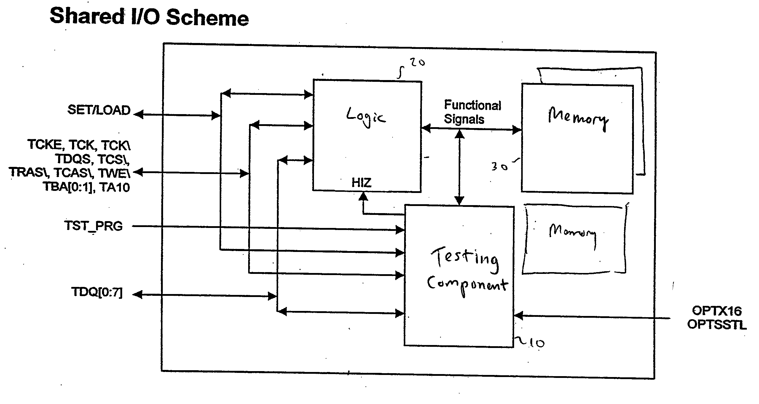
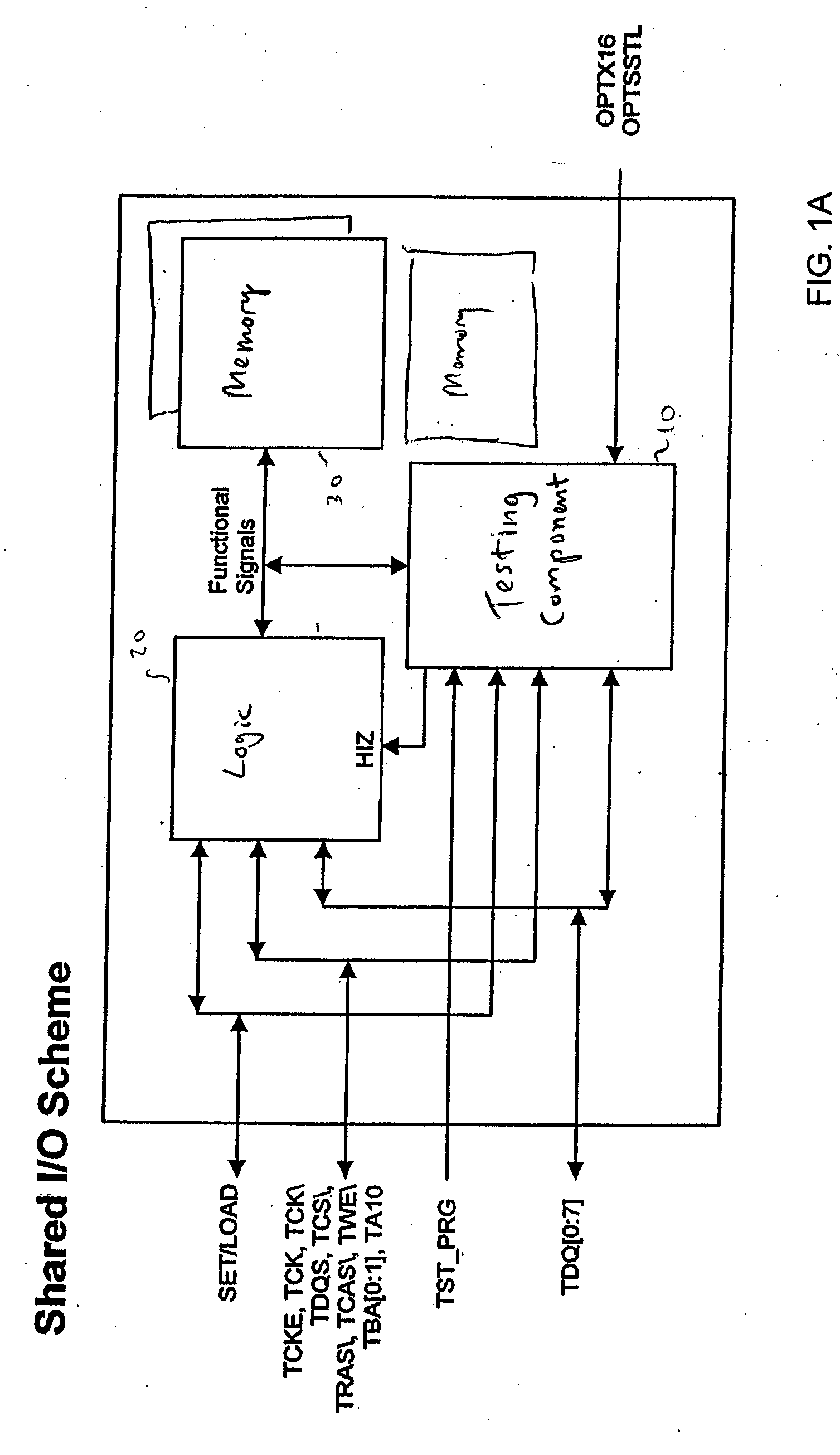
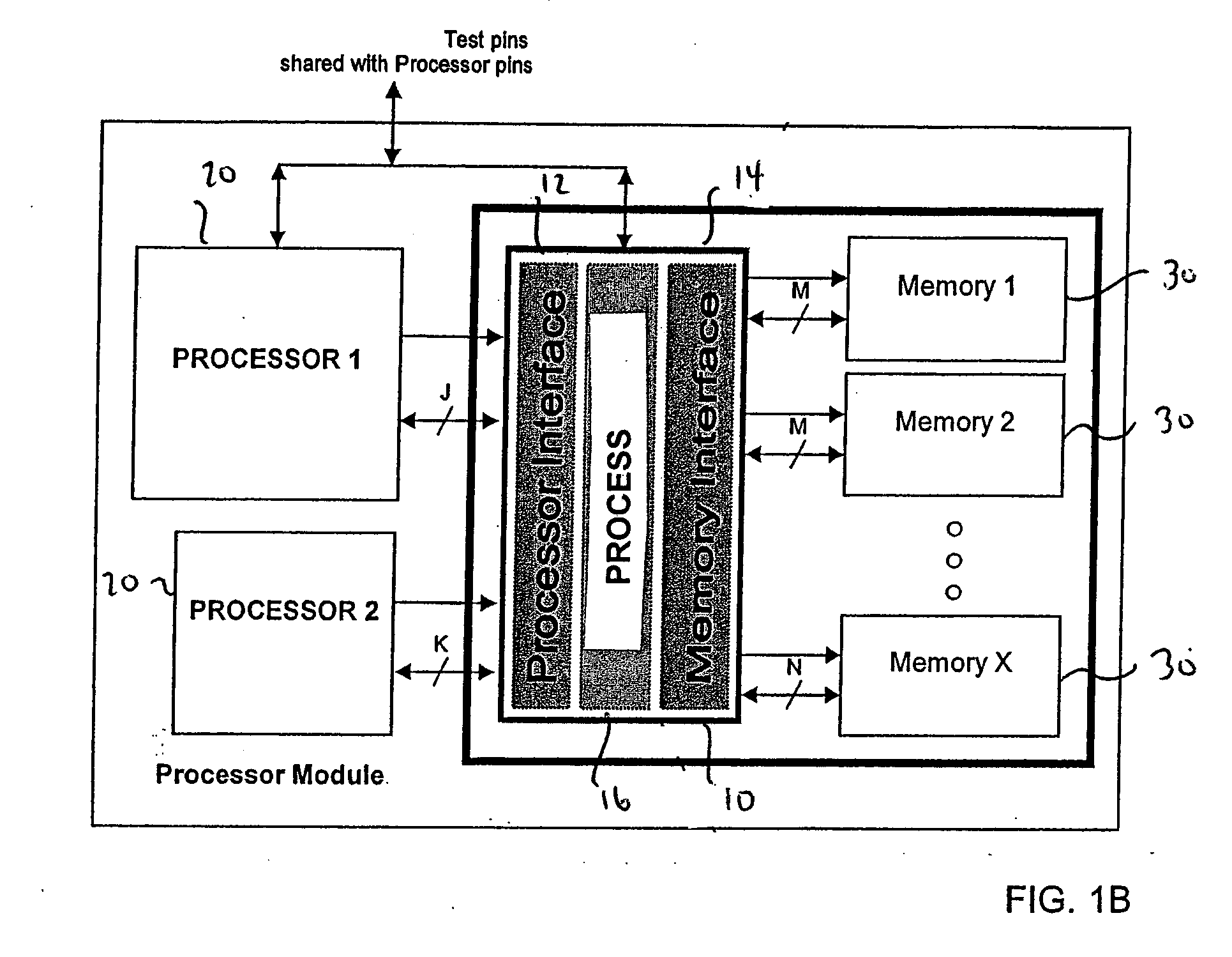
[0026] The preferred embodiments of the present invention and their advantages are best understood by referring to FIGS. 1A through 16 of the drawings. Like numerals are used for like and corresponding parts of the various drawings.
[0027] In one embodiment, the present invention provides a platform of hardware and / or software that enables the complete access and reliable testing of multiple integrated circuit (IC) devices within a package. This platform may include a testing component (e.g., test circuits, test pads, shared pads, etc.), one or more probe cards and related hardware, wafer probe programs, load board and related hardware of external test equipment, and software and routines for final test programs.
[0028] The testing component, in various embodiments, may comprise or specify pad coordinates for complete wafer and package testing; one or more digital test pads (e.g., for TEST, SET, LOAD, TDQ[0:7], or other test command inputs); one or more analog test pads; separate te...
PUM
 Abstract
Description
Claims
Application Information
 - R&D Engineer
- R&D Manager
- IP Professional
- Industry Leading Data Capabilities
- Powerful AI technology
- Patent DNA Extraction
Browse by: Latest US Patents, China's latest patents, Technical Efficacy Thesaurus, Application Domain, Technology Topic.
© 2024 PatSnap. All rights reserved.Legal|Privacy policy|Modern Slavery Act Transparency Statement|Sitemap